
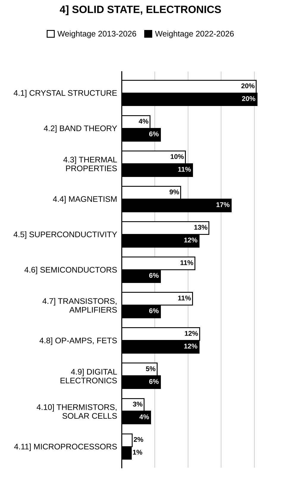
Here are all 218 Solid State Physics, Devices and Electronics questions asked in UPSC Physics Optional Paper II from 1995 to 2026, arranged under the 11 topics of the official syllabus. Within each topic the latest questions come first.
Each question ends with a code such as [2024/15m/3b] – the year, the marks, the word limit (where UPSC set one) and the question number in the paper.
4.1] Crystal structure and its determination
33 questions
(i) What are the different methods used to increase the probability of exposure for the atomic planes with right orientation to X-rays in the X-rays diffraction studies? (ii) Explain the principle and working of the Laue’s diffraction method. Comment on the origin of Laue spots and the utility of Laue’s diffraction pattern. [2026/20m/6c]
Find the radius of the interstitial sphere which can just fit into the void at the body centre of the fcc structure coordinated by the facial atoms. [2025/10m/5c]
In powder diffraction method pattern for lead with radiation of wavelength Å, the (220) Bragg reflection angle is . Find the radius of the atom. [2025/10m/5d]
What is X-ray diffraction? How is an XRD pattern used to determine the crystal structure of the material? [2025/15m/8b]
The spacing between successive (100) planes in sodium chloride is 1.41 Å. X-rays incident on the surface of the crystal are found to give rise to second order Bragg reflections at a glancing angle 10°. Calculate the wavelength of X-ray radiations. [2024/10m/5b]
Derive diffraction conditions using reciprocal lattice concept. What are these conditions known as? [2023/10m/5d]
Considering atoms hard, uniform spheres, find the number of atoms per unit cell and packing fraction for simple cubic, bcc and fcc structures. [2022/15m/6b]
The wavelength of a prominent X-ray line from a copper target is 0.1512 m. The radiation, when diffracted with (111) plane of a crystal with fcc structure, corresponded to a Bragg angle of 20.2°. If the density of the crystal is 2698 kg/m³ and atomic weight is 26.98 kg/k mol, calculate the Avogadro number. [2022/15m/8b]
An X-ray beam of wavelength () undergoes a first order Bragg reflection at a Bragg angle of 30°. X-ray of wavelength 97 nm undergoes 3rd order reflection at a Bragg angle of 60°. Consider that the two beams are reflected from the same set of planes. Find the value of . [2021/10m/5a]
The lattice parameter and the atomic mass of a diamond crystal are 3.57 Å and 12, respectively. Calculate the density of the crystal. Given, Avogadro’s number, . [2020/10m/1e]
Deduce the Miller indices of the close-packed planes of atoms in the f.c.c. lattice. [2019/10m/5c]
The angles between the tetrahedral bonds of diamond are the same as the angles between the body diagonals of a stack of neighbouring cubes having common edges and not faces. Use vector analysis to find the value of the angle. [2019/10m/5d]
Consider a face-centred cubic lattice of side a. Deduce– (i) the primitive translation vectors; (ii) the volume of the primitive cell; (iii) the reciprocal primitive translation vectors; (iv) the volume of the reciprocal lattice. [2019/20m/7a]
Calculate Atomic Packing Fraction (APF) for FCC and HCP structures, and show that these are the most closely packed structures. [2018/10m/5d]
Derive Bragg diffraction law for X-ray diffraction. Compare Laue and Debye-Scherrer methods for crystal structure determination. [2018/10m/5e]
The primitive translation vectors of a two-dimensional lattice are Determine the primitive translation vectors of its reciprocal lattice. [2016/10m/5d]
Obtain Laue’s equations for X-ray diffraction by crystals. Show that these are consistent with the Bragg’s law. [2016/20m/8b]
Show that any arbitrary rotation axis is not permitted in a crystal lattice. [2015/10m/5b]
In a cubic unit cell, find the angle between normals to the plane (111) and (121). [2014/10m/5e]
Explain the working of SEM and TEM and highlight the major differences in principles. Draw neat schematic diagrams. [2014/20m/6a]
What is the reciprocal lattice and why is it named so? Derive the relationships for the primitive translation vectors of the reciprocal lattice in terms of those of the direct lattice. [2014/20m/8a]
.
[Figure: A crystal plane drawn on three mutually perpendicular axes x, y, z meeting at the origin (x towards the lower left, y towards the lower right, z vertically up). Unit lengths a, b and c are marked by dots on the x, y and z axes respectively. The plane is the triangle joining its intercepts: 1a on the x-axis, 3/2 b on the y-axis and 2c on the z-axis.]
A crystal plane is shown in the above figure. Find its Miller indices and interplanar spacing. [2013/10m/5d]
Metallic iron undergoes a structural phase transition from bcc to fcc at 910°C. At this temperature, the atomic radii of iron atoms in the bcc and fcc structures are m and m respectively. Calculate the volume change in percentage during this structural change. [2012/12m/5d]
Derive Bragg diffraction condition in vectorial form using incident and diffracted wave vectors and reciprocal lattice vector. [2011/10m/5b]
An electron beam of 4 keV is diffracted through a Bragg angle of 16° for the first maxima. If the energy is increased to 16 keV, find the corresponding Bragg angle for diffraction. [2011/10m/5d]
Show that the reciprocal lattice of a hexagonal lattice is a hexagonal lattice with a rotation of axes. [2009/10m/5c]
Which of the waves out of (i) X-rays, (ii) de-Broglie waves due to electrons or neutrons will be suitable for crystal diffraction? Justify your answer in terms of energies of these waves for 0.1 nm. [2009/15m/7a]
Show that a lattice cannot have a five-fold rotational symmetry. However, some solids appear to exhibit this rotational symmetry. Explain briefly how this can be done. [2007/10m/5b(i)]
Drawing necessary diagrams, explain diamond structure and CsCl structures. [2006/10m/5d(ii)]
Determines the reciprocal lattice vectors of an fcc lattice. [2005/8m/5b(iii)]
Draw a bcc lattice. Determine its primitive lattice vectors and calculate the packing fraction. [2003/12m/5b(ii)]
Show that for a cubic lattice, the difference between the successive h, k, l planes is given by [2002/10m/5b(ii)]
(i) Obtain reciprocal lattice to normal BCC lattice. (ii) Describe Josephson junction and the effect. How is it exploited in the formation of a SQUID? Write down the applications of a SQUID. (iii) Distinguish between intrinsic and extrinsic semiconductors. Explain the concept of hole. [2001/20m/5c]
4.2] Band theory of solids
16 questions
(i) What is the effective mass of an electron? (ii) What are the physical reasons that the effective mass of an electron can be infinite and negative? (iii) The energy near the valence band edge of a crystal is given by . An electron with wave vector is removed from an orbital in the completely filled valence band. Determine its effective mass and momentum. [2026/10m/5d]
(i) What is the concept of effective mass of the electron? (ii) The energy near a valence band edge is given by ergs. An electron is removed from the orbital . Find the sign and magnitude of effective mass of the hole. [2024/20m/7b]
The energy (E) and wave vector (k) for a conduction band electron in a semiconductor are related as where is a constant and is the free electron mass. Calculate the effective mass of the electron. [2017/10m/5d]
Describe the motion of an electron in one dimensional periodic potential and show that it leads to formation of bands of allowed and forbidden states in the electron energy spectrum. How are the conductors, semiconductors and insulators discriminated on the basis of band structure? [2015/20m/8b]
Starting from an expression for the group velocity, arrive at an expression for the effective mass of an electron in a semiconductor. Explain the significance of sign of the effective mass. [2012/30m/7a]
Explain the origin of energy band formation in solids. Show that in nearly free electron approximation, the energy band gap is , where is Fourier transform of periodic potential seen by the valence electrons. [2011/20m/7b]
Explain the reduced zone scheme of plotting the energy bands in solids. On the basis of E vs k curve distinguish between conductors, semiconductors and insulators. [2010/10m/5b]
What is nearly free electron approximation? On the basis of this approximation explain the formation of energy bands in solids. [2010/20m/7a]
Discuss briefly the concept of effective mass in semiconductors and explain the significance of negative effective mass. [2007/10m/5d(i)]
On the basis of band theory, explain the classification of solids by considering their electrical properties. [2006/10m/5b(ii)]
What are Brillouin zones? How are they related to the energy levels of an electron in a metal? Draw the Brillouin zone for a rectangular lattice of sides π and 2π. Also compute the energy at the corner and midpoints of the adjacent sides of the first Brillouin zone. [2006/30m/7c]
Discuss briefly the concept of effective mass in semiconductors and explain the significance of negative effective mass. [2005/10m/5d(i)]
In isolated atoms, the electrons have discrete and definite energies but in solids they have bands of energies. Explain why. [2005/5m/5d(ii)]
Discuss the motion of an electron in one-dimensional periodic potential and show that it leads to formation of bands of allowed and forbidden states in the electron energy spectrum. How are the insulators, semi-conductors and conductors discriminated on the basis of band structure? [2005/30m/7b]
By drawing E vs. curve, distinguish between metal, insulator and semiconductor. [2004/10m/5b(ii)]
Show that the condition of periodicity of lattice leads to the Bloch theorem. What is a Bloch function? [2004/20m/7c]
4.3] Thermal properties of solids
12 questions
(i) Discuss the Debye model of lattice specific heat. What are the limitations of the Debye model? (ii) At very low temperatures, the specific heat of rock salt varies with temperature according to the Debye law. The Debye temperature for rock salt is 281 K. How much heat will be required to raise the temperature of 2 kilo-mol of rock salt from 10 K to 50 K? [2026/15m/8a]
Derive an expression for the specific heat of a solid based on the Debye theory and show how it agrees with the experimental values. What is the most important assumption of Debye theory in comparison to Einstein theory? Is there any drawback of Debye theory? [2023/20m/7b]
Explain the drawbacks of Einstein’s theory of specific heat and how it was overcome by Debye. [2022/20m/7a]
Using the expression for internal energy show that Einstein specific heat capacity is given by; Also show that Einstein specific heat capacity given above is proportional to at very low temperature. [2021/10m/5b]
Derive the expression for the average energy of a quantum oscillation of frequency v. Assume Fermi-Dirac distribution and , where is the Fermi level. [2019/15m/7b]
Derive an expression for lattice specific heat in Debye model. Find its low temperature limit (Debye law). [2018/15m/7b]
Write down the salient features of the Einstein’s theory of lattice heat capacity. Further write down the expression for specific heat in Einstein’s theory and explain its high and low temperature limits. [2016/10m/8c]
Find an expression for lattice specific heat of a solid, and its low and high temperature limits. What is Debye temperature? [2015/20m/8a]
The velocity of sound in f.c.c. gold and f.c.c. copper is 2100 m/s and 3800 m/s respectively. If the Debye temperature of copper is 348 K, then determine the Debye temperature of gold. Take the densities of gold and copper as and respectively. [2014/10m/5c]
Find an expression for lattice specific heat of solids, and its low and high temperature limits. What is Debye temperature? [2011/20m/7a]
Distinguish between Einstein and Debye models of specific heats of solids. Obtain an expression for the specific heat of a solid on the basis of Debye model. Discuss the results for low and high temperature ranges. [2010/20m/7b]
Derive an expression for the specific heat of a solid on the basis of Debye’s model. Show that it converges to Dulong and Petit’s law at high temperatures. [2009/25m/7b]
4.4] Magnetism
13 questions
(i) What is diamagnetism? Why do diamagnetic materials have negative magnetic susceptibility? (ii) Discuss the limitations of the quantum theory of diamagnetism. (iii) Draw a diagram of magnetic susceptibility as a function of temperature. Pay attention to the relative scales in your diagram so that the relative strengths of the magnetic phenomena are presented. [2026/20m/7a]
Explain the cause of hysteresis phenomenon in ferromagnetic materials. What does the area of the hysteresis loop signify? [2025/15m/7c]
Classify diamagnetic, paramagnetic and ferromagnetic materials in terms of their magnetic susceptibility (). Plot and explain the variation of with temperature for the three materials. [2025/20m/8a]
(i) What is the origin of paramagnetism? Discuss the temperature dependence of paramagnetic susceptibility. (ii) Calculate the diamagnetic susceptibility of atomic Hydrogen in the ground state at STP. Assume the mean square distance of electronic charge distribution of atomic Hydrogen from the nucleus , being the radius of the first Bohr orbit of Hydrogen. [2024/15m/7a]
Explain classical theory of diamagnetism. Show that the susceptibility of diamagnetic substances is directly proportional to the atomic number. Why all the electrons in an atom contribute to diamagnetism? [2023/15m/7a]
A solid contains a dilute concentration of ions, each of which possess three electrons. Assuming that there are of these ions, calculate the magnetic susceptibility of the sample at . [2021/20m/8b]
A system of paramagnetic atoms (N per unit volume) which can occupy only two energy levels in a uniform external magnetic field H is at a temperature T. If this system follows Boltzman’s distribution, find the magnetisation and susceptibility of the system. [2017/20m/7a]
Classify diamagnetic, paramagnetic and ferromagnetic materials in terms of their magnetic susceptibility . Plot and explain the variation of with temperature for the three materials. [2012/15m/7b(i)]
Distinguish between classical and quantum theory of paramagnetism. Explain the paramagnetism of free electrons on the basis of F. D. distribution. [2010/20m/7c]
What are the salient characteristics of ferromagnetic? Explain how the Curie law of paramagnetism is modified to the Curie – Weiss law. [2000/20m/1c]
Distinguish qualitatively between dia-, para-, ferro-, antiferro- and ferrimagnetism. How is the weak and temperature independence paramagnetism of metals explain? [1998/20m/1c]
Assuming that for a paramagnetic material, the magnetic susceptibility is inversely proportional to temperature in Kelvin, obtain Curie-Weiss law for the paramagnetic phase of a ferro-magnetic material. [1997/20m/1c]
How does a ferromagnetic material get magnetized? Why is the demagnetization process irreversible? What is the physical significance of the magnetic hysteresis loop for a ferromagnetic material? Under what conditions the ferromagnetic materials become paramagnetic? [1995/20m/1c]
4.5] Superconductivity
28 questions
Explain briefly the two-fluid model proposed by the London brothers and obtain the expressions for the penetration depth and the number of superelectrons in a superconducting specimen. [2026/10m/5e]
How does supercritical magnetic field depend on temperature? For a superconducting specimen, the critical magnetic fields are respectively A/m and A/m for 14 K and 13 K. Determine the superconducting transition temperature and the critical field at 0 K. [2024/10m/5e]
What is superconductivity? Explain Meissner effect. Why superconductors should be a diamagnetic material? [2023/15m/8b]
Explain why Type-II superconductor is better than Type-I superconductor in the application of superconductor magnets. [2022/10m/5c]
Compare the dependence of resistance on temperature of a superconductor with that of a normal conductor. Describe briefly the formation of Cooper pairs. [2022/15m/7c]
Using the two-fluid model of a conductor (normal and superconducting) and the Maxwell’s equations, derive the two London equations of superconductivity. [2020/20m/4c]
What are type I and type II superconductors? Give examples. Discuss and compare Meissner effect and perfect diamagnetic behaviour for type I and type II superconductors. [2018/20m/8a]
Obtain the expression for penetration depth using London’s equation of superconductivity and explain its significance. [2017/15m/7b]
With the help of a schematic diagram, show how entropy and specific heat vary with temperature for a superconductor. [2016/10m/5e]
Distinguish between a superconductor and perfect conductor. Explain what is a Cooper pair. [2015/10m/8c]
How does the energy gap in superconductors differ from the energy gap in insulator? How does it vary with temperature for superconductors? [2014/10m/5d]
Lead in the superconducting state has critical temperature of 6.2 K at zero magnetic field and a critical field of at 0 K. Determine the critical field at 4 K. [2014/10m/7c]
A perfect conductor and a superconductor with K are subjected to the following conditions: (i) cooled under applied magnetic field to 4 K (ii) cooled to 4 K and then magnetic field is applied with schematic diagrams, explain path of magnetic field lines in all these situations. [2013/15m/7b]
Show that the London equation or leads to the Meissner effect. [2013/15m/7c]
Explain the variation of magnetisation of a type-I and type-II superconductors as a function of applied magnetic field. [2012/15m/7b(ii)]
Describe the characteristic properties of a superconductor. Derive London equation for a superconductor and hence explain Meissner effect. [2011/20m/7c]
What is Josephson tunneling? Distinguish between a.c. and d.c. Josephson effects. [2010/10m/5d]
A type-II superconducting material with superconducting transition temperature is placed in a magnetic field. What is the material state (normal or superconducting or mixed) for (i) (ii) (iii) (iv) (v) where and are the lower and upper critical fields for a type-II superconductor. [2009/10m/5d]
What is Meissner effect? Explain the conclusions drawn from the Meissner effect. [2009/20m/7c]
What is Josephson effect? Discuss briefly DC and AC effects. Give some practical applications of Josephson junctions. [2007/30m/7b]
What are high superconductors? Give two examples indicating their transition temperatures. Differentiate between the conventional and high super conductors. [2003/12m/5d(i)]
What is a Josephson junction? Discuss dc and ac Josephson effects and obtain the relation. where the symbols have their usual meaning. [2003/30m/7b]
Explain Meissner effect and Josephson effect. Describe their applications in the field of superconductivity. [2002/20m/7a]
(i) Obtain reciprocal lattice to normal BCC lattice. (ii) Describe Josephson junction and the effect. How is it exploited in the formation of a SQUID? Write down the applications of a SQUID. (iii) Distinguish between intrinsic and extrinsic semiconductors. Explain the concept of hole. [2001/20m/5c]
(i) Give a qualitative account of BCS theory of superconductivity. (ii) Obtain an expression for conductivity of an intrinsic semiconductor. How does it vary with temperature? (iii) The resistivity of an intrinsic semiconductor is 4.5 ohm-m at 20°C and 2.0 ohm-m at 32°C. Calculate the energy band gap. [2001/30m/7c]
Explain why superconductors are perfect diamagnets. [2000/20m/8c]
What is Meissner effect? Superconducting tin has a critical temperature of 3.7 K in zero magnetic field and critical field at 0 K is 306 gauss. Determine the critical field at 2K. [1999/20m/7b]
Explain the basic distinction between a perfect conductor and a superconductor. [1997/20m/5d]

Preparing for Prelims too?
Our UPSC Prelims Topic-wise PYQ eBook covers every Prelims question with detailed explanations, so you can see exactly where UPSC asks from.
View the BookDownload Free Sample4.6] Semiconductors
24 questions
Show that the Fermi level shifts upward, closer to the conduction band in an -type semiconductor and shifts downward, closer to the valence band in a -type semiconductor. [2023/10m/5e]
Show that for an -type semiconductor, the Fermi level lies midway between the donor states and the conduction band edge at low temperature (assuming ). [2022/20m/8a]
What is an intrinsic semiconductor? Intrinsic silicon has a band gap of 1.1 eV and yet at K, the conductivity is non-zero. Explain. Comment, with the help of relevant expression, on the position of the Fermi level of an intrinsic semiconductor. [2020/15m/6b]
A silicon semiconductor sample at K having cross-sectional area of has a pentavalent donor doping profile given by . Given, the mobility of the electrons in the sample is and the diffusion length of the electrons, , is 4 μm. Calculate the diffusion current in the sample at distance . [2019/10m/5e]
A silicon semiconductor sample is doped with of aluminium and of phosphorus atoms. Given at K, the intrinsic carrier concentration, ; the band gap, eV; the electron mobility, and the hole mobility, . Determine in the sample of the following: (i) The type of the semiconductor, n or p (ii) The hole carrier concentration (iii) The electron carrier concentration (iv) The position of the Fermi level in the sample with respect to the bottom of the conduction band (v) The conductivity of the sample. [2019/20m/8a]
What are intrinsic and extrinsic semiconductors? Show that in the intrinsic semiconductors, Fermi level lies exactly in the middle of bottom of conduction band and top of valence band. [2018/15m/7c]
In a semiconductor, the effective masses of an electron and a hole are and , respectively, where is the free electron mass. Assuming that the average relaxation time for the hole is half of that for the electrons, calculate the mobility of the holes when the mobility of the electrons is . [2017/15m/7c]
What is the difference between direct and indirect band gap semiconductors? Which one is suitable for use in solar cells? [2016/20m/8a]
An electric field of 100 V/m is applied to a sample of n-type semiconductor whose Hall coefficient is . Determine the current density in the sample assuming . [2014/10m/8c]
Starting with the expression for the density of states for electrons in a band, show that the Fermi energy of an intrinsic semiconductor is at the middle of the band gap. Use these results to estimate the electron density at 300 K (Assuming eV and the rest masses of electron and hole as and ). [2013/20m/7a]
Distinguish between intrinsic and extrinsic semiconductors. Show that in a semiconductor, the product of concentrations of the two types of charge carriers is constant at a given temperature. [2011/30m/8a]
Silicon is the most popular semiconductor material used for the fabrication of electronic devices and integrated circuits. Why? Give at least five reasons. [2009/10m/5f]
An In As semiconductor sample is cut in the form of a small bar of size 1.0 cm × 1.0 cm × 2.0 mm. Its lengthwise resistance is 1.25 Ω. A Hall field of 1.7 V/m develops when a current of 0.12 A is passed lengthwise and a magnetic field of 0.05 T is applied normal to its length as shown above. Calculate the carrier density.
[Figure: Printed above the text of (ii): a rectangular bar (cuboid) drawn in perspective, with hidden edges dashed; an arrow labelled I points horizontally to the right along the length of the bar (current lengthwise), and an arrow labelled H points vertically upward from the top face (magnetic field normal to the length).] [2005/6m/5b(ii)]
Discuss the variation of free carrier concentration with temperature for an intrinsic and extrinsic semiconductors. [2002/12m/5c(i)]
(i) Give a qualitative account of BCS theory of superconductivity. (ii) Obtain an expression for conductivity of an intrinsic semiconductor. How does it vary with temperature? (iii) The resistivity of an intrinsic semiconductor is 4.5 ohm-m at 20°C and 2.0 ohm-m at 32°C. Calculate the energy band gap. [2001/30m/7c]
Discuss the different breakdown mechanisms for a reverse biased Zener diode. [2000/20m/4a]
Do these mechanisms have different temperature coefficients? Explain. [2000/10m/4b]
Which one of these mechanisms shows a negative dynamic resistance? Why? [2000/10m/4c]
A Zener diode of 1 W power has a dynamic resistance of 10 mΩ at the breakdown voltage of 3V. What will be the fluctuations in the current through the diode if the voltage fluctuates by 100 mV? What will happen to the diode? Why? [2000/20m/4d]
Phosphorous is doped in a silicon wafer. The impurity concentration is per . If all the donors are active calculate its resistivity at room temperature. The mobility of electrons is . [1999/20m/4a]
A junction diode in series with a parallel combination of a large resistor and a capacitor acts as a linear detector of amplitude modulated waves. Explain the action. [1999/20m/4c]
If is the peak value of the input voltage , calculate the output voltage .
[Figure: Diode–capacitor voltage-multiplier ladder. An a.c. source on the left. From its top terminal the upper line runs through capacitor to a node, then on to a second node, then through a second series capacitor (label printed as , marked “Out”) to a third node and on to the far right. The lower line runs from the bottom of the source to a node, then through capacitor to a second node, on to a third node, then through capacitor to the far right. Four diodes are connected as rungs between the upper and lower lines: from the node after down to the left end of ; from the second upper node down to the node after ; from the node after the upper down to the left end of ; at the far right end joining the end of the upper line to the right end of . and are drawn alike and and alike, with alternating orientation (exact diode directions not clearly legible in the source). is marked by a dimension arrow along the bottom spanning from the left end (source) to the right end of the ladder.] [1998/20m/1d]
Four silicon diodes are connected as shown in Fig. 1. A sinusoidal voltage of amplitude 2 V is applied in the input. What is the waveshape of the output and its amplitude? If the amplitude of the input voltage is reduced to 1 V, what will be the waveshape of the output and its amplitude? Threshold voltage of each diode is 0.6 V.
[Figure: Fig. 1: Two input terminals on the left (labelled “Input”) and two output terminals on the right (labelled “Output”). In the upper line a diode is in series, pointing to the right (anode towards the input terminal, cathode towards the output side); in the lower line an identical series diode, also pointing to the right. Between the upper and lower lines, on the output side, two diodes are connected in parallel as shunt elements: the first (left) points downwards (anode on the upper line, cathode on the lower line); the second (right) points upwards (anode on the lower line, cathode on the upper line). The output is taken across this anti-parallel pair.] [1997/20m/1d]
How does built in potential appear across a p-n junction? Explain under what biasing conditions drift and diffusion currents, respectively, dominate. [1995/20m/1d]
4.7] Transistors, amplifiers and oscillators
30 questions
An RC-coupled transistor amplifier has mid-frequency gain . The values of the lower and upper cut-off frequencies are Hz and kHz. Find the frequencies at which the gain is reduced to 80. [2024/15m/7c]
With a neat circuit diagram, explain the working of Wien-Bridge oscillator. [2023/15m/7c]
An –– transistor with is used in common-emitter amplifier mode with and . If a 100 kΩ resistor is connected between the collector and the base of the transistor, calculate the quiescent collector current. Assume . [2021/20m/7a]
Sketch the dc load line for the circuit shown.
[Figure: Fixed-bias common-emitter n-p-n transistor circuit: supply = +20 V at the top rail; collector resistor = 10 kΩ from the rail to the collector, with collector current marked flowing down into it; base resistor (no value given) from the rail to the base, with base current marked flowing into the base; emitter connected to ground; marked between base (+) and emitter (−) and between collector (+) and emitter (−).] [2021/10m/8a]
Consider an amplifier with an open-loop (no feedback) gain of A and a feedback factor . Derive the expression for the gain with feedback, . Derive the condition for the amplifier with feedback to act as an oscillator. Comment on the change in with a change in A. [2020/15m/6c]
An amplifier in common-emitter configuration is shown in the above figure. If the current gain and the a.c. emitter resistance = 25.0 , determine the input impedance and the voltage gain of the amplifier.
[Figure (printed above the text of the part): Common-emitter amplifier with an NPN transistor and supply +9 V. The collector is connected to +9 V through a 2.5 kΩ collector resistor; the output is taken between the collector and ground. The base is biased by a voltage divider: 10 kΩ from +9 V to the base and 10 kΩ from the base to ground. The input (between the input terminal and ground) is applied to the base through a 1 kΩ series resistor. The emitter is connected to ground through a 4.3 kΩ resistor, which is bypassed by a capacitor C (from emitter to ground).] [2017/15m/8a]
Differentiate between n-p-n and p-n-p transistors. Give their device structure and biasing circuits when used as an amplifier. [2015/10m/5e]
Design a transistor based Colpitt oscillator which can oscillate at 9 MHz. Explain how the oscillations are created and sustained. [2015/15m/7a]
Draw and explain the collector characteristics of a bipolar junction transistor in common emitter configuration. Using the plot, explain how the transistor can be used as an ON-OFF switch. [2013/10m/5e]
.
[Figure: Tank circuit: two capacitors = 70 pf and = 20 pf connected in series in the left vertical branch, in parallel with an inductor L = 20 μH in the right vertical branch; output terminals taken from the middle of the top wire and the middle of the bottom wire (the junction between and is not brought out).]
Explain how the circuit shown above can be a source of oscillations. Use this circuit to construct a transistor oscillator and explain its working. What is the frequency of oscillations of this circuit? [2013/25m/8a]
What are the rules followed in biasing a bipolar junction transistor when it is used as an amplifier? Show how n-p-n and p-n-p transistors to be used as an amplifier are biased and the direction of flow of base, collector and emitter currents. [2012/12m/5e]
Draw the common-base amplifier circuit, using an n-p-n transistor and briefly discuss its working. [2011/15m/8c]
Draw a two stage RC coupled transistor amplifier. Plot the frequency response and indicate the lower and upper cut off frequencies and the bandwidth. [2010/30m/8a]
What do you understand by early effect in bipolar junction transistors? What are its consequences? Discuss briefly the advantage of using the BJT in the common collector configuration. [2009/20m/8c]
Explain the difference between n-p-n and p-n-p transistors. Give their device structure and biasing circuits. Draw a circuit for a single-stage common-emitter amplifier. [2007/10m/5c(ii)]
Explain the working of a phase-shift oscillator. Draw the circuit diagram of a phase-shift oscillator using either a transistor or an op-amp. What are the conditions which must be satisfied to achieve stable oscillations? Calculate the frequency of oscillations for and . [2007/25m/8a]
The transistor in the following circuit has β = 100 and V. What value of will give 0 volt d.c. output?
[Figure: Emitter-follower (common-collector) circuit with an n-p-n transistor. Collector connected directly to the +12 V rail. connected from the +12 V rail to the base. Input applied (input terminal, with a grounded return terminal) through a series coupling capacitor to the base. Emitter connected to the output terminal (output taken between emitter and ground) and through = 1.2 kΩ to the −12 V supply. Label: V.] [2006/10m/5c(ii)]
The following common-emitter amplifier is required to have a signal voltage gain of at least 100. The transistor has β = 63, early voltage V and A: Assuming that the operating collector voltage is supposed to be + 6 V, perform related calculations to check whether the circuit satisfies the operating point and voltage gain criteria. The reactance of the capacitors can be neglected at all frequencies.
[Figure: Common-emitter amplifier with an n-p-n transistor. Signal source in series with = 600 Ω, coupled through a series capacitor to the base. = 810 kΩ from the top (supply) rail to the base; = 6.8 kΩ from the top rail to the collector; the supply voltage is not labelled. Emitter connected directly to the common bottom (ground) line, which also returns and . Collector connected to the load = 10 kΩ (a small element on this connection, probably a coupling capacitor, is hidden by the watermark [?]); taken across (arrow pointing up).] [2006/20m/8a]
Define α and β parameters of a transistor. A germanium transistor with is biased as shown above. Calculate the value of .
[Figure: Printed above the text of (ii): collector-feedback bias circuit of an npn transistor (emitter arrow pointing outward). Supply V at the top connects through a 10 KΩ collector resistor to the collector. The base resistor is connected between the collector node (below the 10 KΩ resistor) and the base. The emitter goes through a 300 Ω resistor to ground. A dimension arrow between two dashed horizontal lines drawn level with the collector node and the emitter node is marked 5 V (i.e. collector–emitter voltage 5 V).] [2005/8m/5c(ii)]
Discuss the functioning of the above oscillator circuit. Obtain the condition for maintenance of oscillations and the expression for the frequency assuming that the resistances of the inductors are negligible.
[Figure: Printed before the text of (b): transistor Hartley oscillator (npn transistor). Vcc at the top feeds two branches: through resistor down to the base node, and through an RFC (radio-frequency choke) down to the collector. Resistor runs from the base node down to the bottom of the emitter network. The emitter goes through shunted by capacitor to a node that is connected to ground. The tank circuit at the bottom: two inductors (left) and (right) in series with their common junction grounded; a variable capacitor C is connected across the outer ends of and . The base is coupled through capacitor to the outer (left) end of , and the collector is coupled through capacitor to the outer (right) end of .] [2005/30m/8b]
A transistor with , [?] V, V and is used in biasing circuit as shown in the figure. It is designed to establish the quiescent potential at V, [?] mA and stability factor . Find the values of resistors , and , where symbols have their usual meanings.
[Figure: Voltage-divider bias circuit of an npn transistor. A +22.5 V supply line at the top; from the supply line to the base node and from the base node to ground; from the supply line to the collector; the emitter (current , arrow pointing out of the emitter) goes to ground through .] [2004/20m/5c]
Draw a circuit diagram of an R-C phase shift oscillator. Explain its working. Derive an expression for its frequency. [2004/30m/8a]
Explain the principle of feedback in an amplifier. What are the advantages & negate feedback? [2003/8m/5d(ii)]
Derive the various current components in a p-n-p transistor when it is actively biased. Using Ebers-Moll model, show that for the common-emitter configuration where the symbols have the usual meaning. [2003/30m/8a]
In the following circuit, Show that the stability factor, S, is given by Where
[Figure: Printed between “is given by” and the formula: voltage-divider (potential-divider) bias circuit of an npn transistor. from to the base node and from the base node to the common (ground) line; the input is coupled to the base through a capacitor. The collector goes to through , and the output is taken from the collector through a coupling capacitor. The emitter goes to the common line through shunted by a bypass capacitor .] [2003/20m/8b]
Explain the effect of negative and positive voltage feedback on an amplifier characteristics. [2002/8m/5c(ii)]
Explain the working N-P-N transistor. Derive expression for the current and voltage gains. [1998/20m/4a]
Draw the circuit of an emitter-follower and find its voltage gain. [1997/30m/4a]
A Si BJT is connected as shown Fig. Show that it is in active region and works as an amplifier Calculate its mid frequency gain, given that BJT has . , = [?], nA.
[Figure: Common-emitter BJT (npn) amplifier with voltage-divider bias. Supply +15 V. Base bias divider: 54 k from +15 V to the base and 12 k from the base to ground. Collector resistor 3 k from +15 V to the collector, with collector current marked mA flowing down through it. Emitter resistor 1 k from the emitter to ground. No coupling or bypass capacitors and no input/output terminals are shown.] [1996/30m/4b]
Establish the two Barkhausen conditions for sustained sinusoidal oscillations. Sketch the circuit of Wien’s bridge oscillator and explain its working. [1995/30m/4a]
4.8] Op-amps and field effect transistors
25 questions
The input signal as shown in Figure (I) is applied to the comparator circuit given in Figure (II). Make a sketch of the output signal showing its proper relationship to the input signal. Assume that the maximum output levels of the op-amp are V.
[Figure: (I) Input signal versus time t: a sine wave starting at zero, rising to a positive peak of 5 V, crossing zero and falling to a negative peak of –5 V, then returning to zero (one full cycle); levels 5 V and – 5 V marked on the vertical axis. (II) Comparator: an op-amp whose inverting (–) input is connected to the junction of a voltage divider formed by = 8.2 kΩ (from the + 15 V supply to the junction) and = 1.0 kΩ (from the junction to ground); the input is applied to the non-inverting (+) input (its wire crosses the divider wire below the junction without connecting); output .] [2026/10m/7b]
What are the differences in electrical characteristics of FET (JFET) and MOSFET? [2025/7m/5e(i)]
How does -channel FET differ from -channel FET? [2025/3m/5e(ii)]
Compare the working of FET and MOSFET with their structure, I – V curve and transfer characteristics. [2024/15m/8c]
Determine the input and output impedances of the amplifier in given figure. The op-amp datasheet gives , and (open loop voltage gain).
[Figure: Non-inverting op-amp amplifier: input (terminal) connected to the non-inverting (+) input of the op-amp; output terminal taken from the op-amp output. A feedback resistor is connected from the output down to a junction node, and a resistor from that node to ground; the node between and is connected back to the inverting (−) input.] [2023/10m/8c(i)]
Find the closed-loop voltage gain. [2023/5m/8c(ii)]
Why is the Field Effect Transistor (FET) called Unipolar Transistor? Discuss how it is superior than Bipolar Junction Transistor. [2022/10m/5d]
Calculate the pinch-off voltage for -channel silicon FET with a channel width of cm and a donor concentration of . Given that dielectric constant of silicon is 12. [2021/10m/7c]
Sketch the cross-sectional structure of an enhancement mode MOSFET and explain its principles of operation with the help of its output characteristics. [2019/15m/7c]
What are operational amplifiers? How can it be used as an inductor? Prove it mathematically. [2018/15m/8b]
Consider the operational amplifier circuit given above: Given, , and the product of the open loop gain of the amplifier and its bandwidth = Hz. Determine the closed loop bandwidth of the amplifier.
[Figure (printed above the text of the part): Non-inverting op-amp amplifier. The signal “Input” terminal is connected directly to the non-inverting (+) input of the op-amp. Resistor connects the inverting (−) input to ground; resistor is the feedback resistor from the op-amp output to the inverting (−) input. The op-amp output terminal is labelled “Output”.] [2017/10m/5e]
Given above is a circuit of self biased p-channel JFET. If the pinch off voltage is 5.0 V and = 6.0 V, calculate the saturation current .
[Figure (printed above the text of the part): Self-biased p-channel JFET (gate arrow pointing outward from the channel, labelled G). The drain D is connected through a 2 kΩ resistor to a −12 V supply; the source S is connected to ground through a 1 kΩ resistor; the gate G is connected to ground through a 5 kΩ resistor. Polarity marks between drain and source: “−” at the drain side and “+” at the source side.] [2017/15m/8b]
Describe an operational amplifier based integrator. Using operational amplifier integrators, design a circuit to solve the following differential equation: [2015/20m/7b]
Give the basic structure of n-channel depletion type MOSFET. Draw the drain current-drain voltage characteristics both in depletion as well as enhancement modes. [2014/20m/6b]
Construct an operational amplifier based analog computer to solve the differential equation [2012/30m/8a]
Identify the above op-amp circuit. Estimate the net output voltage .
[Figure (printed above the text of part (f)): Op-amp circuit. A 2 V source (battery, + terminal up, − terminal grounded) is connected through a 10 K resistor to the inverting (−) input, pin 2, of the op-amp. A 20 K feedback resistor connects the output, pin 6, back to the inverting input (pin 2). The non-inverting (+) input, pin 3, is connected directly to the + terminal of a second 2 V source whose − terminal is grounded. Supply pins: pin 7 to +15 V, pin 4 to −15 V. The output at pin 6 is .] [2010/10m/5f]
Give the basic structure of a n-channel depletion type MOSFET. Draw the drain current–drain voltage characteristics both in depletion as well as in enhancement modes. [2010/15m/8b]
List the characteristics of an ideal OP-AMP. Write the expression for the output voltage in terms of input voltages and resistance values.
[Figure: Inverting summing amplifier. Three input terminals , , are connected through resistors , , respectively to a common junction, which goes to the inverting (−) input of the op-amp. A feedback resistor connects the op-amp output back to the inverting input. The non-inverting (+) input is connected to the common (ground) line running along the bottom of the circuit from a ground input terminal to the lower output terminal. The output voltage is taken between the op-amp output terminal and the common line (arrow between the two output terminals).] [2009/20m/8a]
Explain the working and applications of a FET. [2006/20m/8b]
Define (i) input bias current, (ii) input offset current, (iii) input offset voltage, (iv) output offset voltage, (v) power supply rejection ratio and (vi) slew rate for an OPAMP. [2005/30m/8a]
The following information is included on the data sheet for an N-channel JFET: mA, V and . Determine the value of drain current and trans-conductance at V. [2004/10m/5d(i)]
Calculate the gain of the following amplifier circuit: Given that mV/A, and .
[Figure: Printed before “Given that”: a FET amplifier (MOSFET symbol in a circle). The drain is connected to a −24 V supply through the load ; the source is connected to the common (ground) line; the gate is driven by an a.c. signal source (circle with ~) in series with a d.c. bias battery returning to the common line. The output voltage is taken between the drain and the common line.] [2003/10m/8c]
What are the main applications of JFET? Discuss their advantages over bipolar transistors. Explain the working of n-channel JFET with the help of a schematic diagram. [2002/30m/8a]
Write down the characteristics of an ideal operational amplifier. Explain the term virtual ground. Draw a circuit diagram showing virtual ground in an operational amplifier. [2002/30m/8b]
(i) FETs have unique properties which make BJTs not suitable for some important applications. What are these most important FET applications? (ii) Briefly describe FETs as variable resistors. [2001/20m/5d]
4.9] Digital electronics
26 questions
How is digital system different from analog system? What are the principal reasons for the widespread use of digital electronics? [2024/8m/8b(i)]
Give logic diagram, Boolean equation and truth tables of AND, OR and NOT gates. Show that NAND and NOR gates can be utilized as a Universal Gate. [2024/12m/8b(ii)]
Why NAND and NOR gates are called universal gates? Give the logic diagram, Boolean equation and the truth table of a X–OR gate. [2022/10m/5e]
Why are NAND and NOR gates called universal gates? Give the logic diagram, Boolean equation and the truth table of a NAND gate. [2016/10m/5b]
Simplify the logical expression . [2015/10m/5d]
Construct a digital circuit to add three bits A, B and C and provide their sum and carry as outputs. Show appropriate Boolean expressions and truth table to justify the outputs. [2013/25m/8b]
Explain the race problem encountered in an RS latch and how it can be avoided. Build a Mod-10 counter using JK flip-flops and explain its working. [2012/30m/8b]
Simplify the logical expression using a Karnaugh map. [2011/10m/5f]
Simplify the logical expression and draw the logical circuit to implement it. [2011/15m/8b]
Why NAND and NOR gates are called universal gates? Give the logic diagram, Boolean equation and the truth table of a NAND gate. Design an OR gate using only NAND gates. [2010/15m/8c]
Verify that the circuit shown below is an exclusive OR.
[Figure: Logic circuit of four two-input NAND gates with inputs A and B and output Y. Gate 1 has inputs A and B; its output is labelled . Gate 2 (upper) has inputs A and ; its output is labelled . Gate 3 (lower) has inputs and B; its output is labelled . Gate 4 has inputs and ; its output is Y.] [2009/10m/5e]
Simplify the equation: using Boolean algebra Give the logic circuit for the equation before and after the simplification. [2007/10m/5c(i)]
Give the Boolean expression and the truth table for an XOR gate. Why are NAND gates called universal gates? Realise OR and XOR gates employing only NAND gates. [2007/15m/8b]
Simplify the logical expression by using Karnaugh map and realise f using NAND gates only. [2006/10m/5c(i)]
Draw the logic circuit for the following Boolean expression: What are the ‘Y’ values for the input combinations: (1) 1, 1, 0; (2) 1, 0, 1; (3) 0, 0, 1? [2005/12m/5c(i)]
Give the two forms of the De Morgan’s theorem. [2004/10m/8b]
What is the principle used in ‘half-adder’? Give the truth table for it. [2004/20m/8c]
Explain the operation of the following circuit is a gate. Draw the truth table and find the operation carried out by this gate neglecting the source impedance.
[Figure: Diode–transistor logic gate. Three inputs A, B and C, each connected through a diode D to a common node P; the diodes are drawn with their cathodes towards the inputs (anodes at P). An input waveform stepping from 0 V up to 12 V is drawn beside the inputs. Node P is connected to +12V through a 15K resistor. From P a resistor R1 (15K), shunted by a speed-up capacitor C1, goes to the base of transistor Q; the base is also connected to −12V through a 100 K resistor. Q is an npn transistor with its emitter to ground and its collector (C) connected to +12 V through a 2.2 K resistor; the output Y is taken from the collector.]
junction saturation voltages and diode voltages in forward direction. Find the minimum value of . [2003/20m/5c]
Show that a negative logic OR gate is like a positive logic AND gate. [2002/10m/5d(i)]
Combinational switching circuit can perform an addition of the numbers held in two registers. (i) Write down the math table for the addition of two bits. (ii) Write down a Boolean expression for the necessary circuit functions. (iii) Arrive at the Exclusive-OR function. (iv) Draw the logic diagram for the circuit which performs the addition. [2001/10m/8a]
(i) What are sequential switching circuits (ii) Describe a simple sequential circuit. (iii) Describe a clocked RS Flip-Flop, (iv) Briefly describe ROMs. [2001/40m/8b]
A circuit of a NOT gate is given in the figure below. Explain how you will determine the values of the resistances , R and .
[Figure: Single-transistor (npn, common-emitter) NOT gate. Input : a rectangular pulse of height 5 V applied between ground (o) and the input terminal; input connected through series resistor to the base. From the base node a resistor R goes down to a –5 V supply. Collector connected through load resistor to the +5 V supply; output taken from the collector. Emitter (arrow outward) connected to ground.] [2000/20m/1d]
Simplify the given Boolean expression and draw the corresponding logic circuit using NAND gates: [1999/20m/1d]
Simplify the following logic function and draw the corresponding logic diagram:- [1998/20m/4b]
Simplify the following logic function and draw the corresponding logic gates: [1997/30m/4b]
Define ex-OR. Give its truth table and draw the possible logic blocks. [1996/30m/4a]
4.10] Thermistors and solar cells
8 questions
What is the photovoltaic effect? What are the processes that are required to obtain a useful power output from photon interactions in a semiconductor? List the factors that affect the efficiency of a solar cell. [2026/15m/8b]
(i) What is a microprocessor? Describe the internal functioning of a microprocessor with block diagrams. (ii) How do thermistors and solar cells differ in structure and operation? [2025/15m/8c]
A Ge solar cell with a dark reverse saturation current of 2 nA has solar radiation incident upon it, producing electron-hole pairs per second. The electron and hole diffusion lengths are given to be 5 μm and 2 μm, respectively. Calculate for the cell of the following: (i) The short-circuit current (ii) The open-circuit voltage. [2019/10m/8b]
Draw the device structure of a p-n junction solar cell and explain how light energy is converted into electrical energy. Draw and explain its I-V characteristics. [2015/15m/7c]
The resistance of silicon and germanium varies with temperature. But these are not used normally as thermistors. Why? Name at least two widely used materials for making thermistors and give any five applications of thermistor. [2009/20m/8b]
Draw the device structure of a p-n junction solar cell and explain how the light energy is converted into electrical energy. Define the ‘short-circuit current’, ‘open-circuit voltage’ and ‘efficiency’ of a solar cell. [2007/20m/8c]
Explain a solar cell employing its characteristics on output quantity versus quantities like load current, radiance and temperature. [2001/10m/8c]
What is the photovoltaic mode of operation for a photo-diode? Describe the construction and working of a silicon solar cell. [1998/20m/4c]
4.11] Microprocessors and digital computers
3 questions
(i) What is a microprocessor? Describe the internal functioning of a microprocessor with block diagrams. (ii) How do thermistors and solar cells differ in structure and operation? [2025/15m/8c]
Describe the working of a microprocessor system in block diagram. How is its performance affected in a pipelined processor? [2018/15m/8c]
What is a microprocessor? Explain the internal architecture of an 8085 μP. [2006/20m/8c]

Strengthen your GS papers
Our UPSC Mains Topic-wise & Year-wise PYQ eBook (2013–2026) maps every GS question to the syllabus, so you know what UPSC asks and how often.
View the BookDownload Free Sample« Previous: Nuclear and Particle Physics | Next: Other Questions »
Back to: Physics Optional PYQs – Topic-wise
Last updated: 30 October 2026