
Here are all 106 Microprocessors and Microcomputers questions asked in UPSC Electrical Engineering Optional Paper II from 1995 to 2026, arranged under the 4 topics of the official syllabus. Within each topic the latest questions come first.
Each question ends with a code such as [2024/15m/3b] – the year, the marks, the word limit (where UPSC set one) and the question number in the paper.
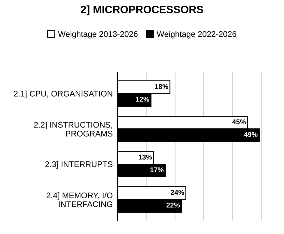
2.1] PC organisation and CPU
21 questions
In the 8085 microprocessor, explain the functionality of the following pins, and describe the role of the instruction decoder, stack pointer and program counter. 1. READY 2. SID 3. SOD 4. INTR 5. CLK (OUT) [2026/10m/2b(i)]
For the instruction MVI B, 05H, draw the timing diagram, if the opcode is stored at 220AH and data at 220BH locations. Incorporate all the control and status signals involved in the operation during the execution. Assume the opcode is XXH. [2026/10m/2b(ii)]
Show an instruction cycle with possible machine cycles and clock cycles (T-states) in it, for the microprocessor 8085. If the processor is working at 3 MHz, calculate the minimum and maximum possible execution time for an instruction. [2022/10m/1c]
(i) Explain the use of MAR in interfacing the external memory to processor. (ii) Name various 8-bit and 16-bit internal registers in microprocessor 8085 and also, indicate which 8-bit registers can be paired to act as 16-bit register in several instructions. [2022/10m/3c]
(i) Name various registers in 8085 microprocessor. Which of these registers are of 16-bit length? (ii) Explain indirect addressing modes in 8085 microprocessor with suitable example. [2020/10m/2c]
Explain the function of the following signals in 8085 microprocessor: (i) ALE (ii) (iii) (iv) [2019/10m/1e]
What is a jump-on-reset circuit in a processor? [2017/5m/5b(ii)]
Assume that the accumulator contains data byte 82H and the instruction MOV C, A (4FH) is fetched. List the steps in decoding and executing the instruction. [2016/10m/7b(i)]
What is pipelining? Explain how it improves the performance of a processor. Discuss how BRANCH like instructions can be handled in a pipelined system. A machine language program has instructions, each having parts. Suppose each part can be executed in one cycle and there is no BRANCH like instruction in the program. How much time does a processor (i) with pipelining and (ii) without pipelining take to execute the program? [2015/20m/2b]
Discuss the role and purpose of the three buses—address, data and control. Explain how they connect microprocessor CPU to ROM, RAM and I/O for data transfer. [2015/10m/4a(ii)]
Specify multiplexed and non-multiplexed bus lines in 8085 microprocessor. [2014/4m/1b(ii)]
Explain hardware single stepping used in 8085 microprocessor. [2014/20m/7b]
Draw the block diagram indicating the typical architecture of a microcomputer. Briefly discuss the salient features. [2013/5m/1c(i)]
Draw the timing diagram for memory read cycle and memory write cycle and explain the significance of the time periods therein. [2013/10m/4b]
List the features of 8086’s segmented memory. [2013/5m/7b(i)]
The instruction OUT FFH of 8085 is stored from memory location 4048 H. The opcode for OUT instruction is D3H. Draw and explain the timing diagram for the execution of this instruction giving timings for signals like ALE, Address lines, data lines and memory. [2009/20m/1c]
What is the difference between a microcomputer and a micro-process? What type of data is stored in the memory of a microcomputer? How much memories can a typical 8-bit micro-process access? What are the condition flags and why are they important? Write the advantage of the indexed address mode compared to the direct addressing mode. Draw the time diagram of out instruction for 8085 micro-process. [2007/20m/2a]
Differentiate between Instruction Cycle (IC) and Machine Cycle (MC), Explain all the basic Machine Cycles of 8085 microprocessor. Explain difference between a FETCH cycle and an INTA signal. [2006/20m/4a]
Discuss briefly the architecture of 8086 microprocessor with special reference to the following (i) Memory organization (ii) Register structure (iii) Addressing modes. [2003/20m/3a]
Discuss briefly the microprocessor architecture with special reference to the following components- (i) Data bus, (ii) Address bus and (iii) Control bus. [2002/20m/3a]
Discuss the functions of various Registers and ALU of 8085. [2000/20m/7a]
2.2] Instruction set and programming
44 questions
Upon execution of the following routine, find the value stored at location 00FFH. MVI B, 0FH MVI C, ABH MOV A, C ADD B SBI 02H STA 00FFH Also write the status of each flag after completion of execution. [2026/10m/1b]
Explain the operation performed by 8085 microprocessor when the following instructions are executed: (i) JMP unconditionally (ii) POP (iii) PUSH (iv) RET (v) STC. [2025/10m/1b]
For 8085 microprocessor, write the instructions to perform the following: (i) Set the zero flag when a register pair is used as a down counter (ii) Load the accumulator with the contents of location 2050H, if memory location 2050H contains byte F8H (iii) Load 3AH in memory location 2050H, if registers H and L contain 20H and 50H (iv) Subtract 25H with borrow from accumulator, if the accumulator contains 37H and the borrow flag is set (v) Complement the accumulator, which has data byte 89H. [2025/20m/2b]
For 8085 microprocessor, write a program to do the following: 1. Clear the accumulator 2. Add 47H (using ADI instruction) 3. Subtract 92H 4. Add 64H 5. Display the results after subtracting 92H and after adding 64H Specify the answer you would expect at the output port. Also give the reason for clearing the accumulator before adding the number 47H directly to the accumulator. [2025/10m/4b(i)]
Write the instruction to clear the CY flag to load FFH in register B and increment (B). If the CY flag is set, display 1 at the output port; otherwise, display the contents of register B. Explain your result. [2025/10m/4b(ii)]
Explain the operation performed by 8085 microprocessor when the following arithmetic instructions are executed: (i) ADD M (ii) ADC M (iii) DAD rp (iv) SBI d8 (v) DCR reg. [2024/10m/1b]
Write an assembly language program to add two numbers of 8-bit data stored in memory locations 4200H and 4201H and store the result in 4202H and 4203H. [2024/10m/3c]
Identify and explain briefly the addressing modes of 8085 microprocessor in the given instructions: (i) ADD reg (ii) MOV rd, M (iii) CALL addr 16 (iv) LDA addr 16 (v) CMA. [2024/20m/4b]
Briefly explain the following logical instructions of 8085 microprocessor: (i) ANA M (ii) XRA M (iii) CMC (iv) STC (v) RRC. [2023/10m/1d]
Discuss with example how BCD number addition is performed using DAA instruction of 8085 microprocessor. [2023/10m/3b(ii)]
Write an 8085 assembly language program to read and complement the contents of the flag register. [2023/8m/6b(ii)]
Explain each step of the assembly language program given below for microprocessor 8085 and calculate the total time taken by the processor in its execution if the processor is working at 3 MHz. (The number of clock cycles for instructions is given in the table for reference): LXI SP, 5000 H; LXI D, 00F9 H; CALL SUBROUTINE 1; HLT; SUBROUTINE 1: DCX D; MOV A, D; ORA E; JNZ SUBROUTINE 1; RET.
| Instruction | Clock cycle |
| LXI | 10 |
| CALL | 18 |
| DCX D | 6 |
| MOV A, D | 4 |
| ORA E | 4 |
| JNZ | 7/10 (for Z=1 or 0) |
| RET | 10 |
[2022/20m/2b]
Explain the following related to computer programming: (i) Machine Language (ii) Assembly Language (iii) Compiler (iv) Interpreter (v) ASCII. [2021/10m/1c]
List the functional classification of 8085 instruction set. Give one example for each class. [2021/10m/5e]
Explain briefly the following control instructions of 8085 microprocessor: (i) HLT (ii) EI (iii) DI (iv) RIM. [2020/10m/1b]
(i) Name various registers in 8085 microprocessor. Which of these registers are of 16-bit length? (ii) Explain indirect addressing modes in 8085 microprocessor with suitable example. [2020/10m/2c]
(i) For 8085 microprocessor, write a program to do the following: (1) Load the number 30H in register B and 39H in register C (2) Subtract 39H from 30H (3) Display the answer at Port 1 (ii) Find the output displayed at Port 1. [2020/10m/3c]
(i) For an 8085 microprocessor program, the instructions are as follows:
| Opcode | Operand |
| MVI | B, 91H |
| MVI | C, A8H |
| MOV | A, B |
| ORA | C |
| OUT | Port 1 |
| HLT |
Determine the output at Port 1, with the explanation of each statement. (ii) For an 8085 microprocessor program given below
| Label | Opcode | Operand |
| Loop: | MVI | B, 64H |
| NOP | ||
| DCR | B | |
| JNZ | Loop |
find the number of times the loop will be executed. [2020/10m/6c]
Write an assembly language program using the instruction set of 8085 microprocessor for addition of six bytes of data stored in memory locations starting at 2050H. The carry generated (if any) must be saved in register B. The entire sum must be stored at two memory locations 2070H and 2071H. [2019/10m/5d]
Write an 8085 microprocessor assembly language program to turn ON an LED connected to bit 4 of the 8155 I/O port B. Use address of port B as . [2018/10m/2c]
Differentiate between the following pairs of instructions: (i) LDA addr and STA addr (ii) LDAX rp and SHLD addr (iii) LDAX rp and STAX rp (iv) RLC and RAL (v) PCHL and SPHL. [2018/10m/4c]
Explain five addressing modes of 8085 microprocessor. [2018/10m/6c]
In an 8085 microprocessor, what is the value of stack pointer after the following program is run?
| MOV | SP, 07FFH |
| PUSH | B |
| CALL | Subroutine |
| POP | B |
| ADD | B |
| PUSH | B |
| HLT |
[2017/5m/7b(i)]
Write down the ALP (Assembly Language Program) to exchange 10H data bytes stored from memory location 2450H with data bytes stored from memory locations 2480H onwards. [2016/10m/5c]
Describe the function of each of the following mnemonics. How many cycles do each of them require for execution and which are the flags affected? Explain. 1. DAD (Double Add) 2. CMC (Complement Carry) 3. LHLD (Load H-L Register Pair Direct) 4. ORI (OR Immediate) [2016/10m/7b(ii)]
Discussing the issues in memory addressing, explain the five addressing modes used in 8085. [2015/10m/1e]
Briefly discuss the functional classification of the instruction set, explaining role and format of instructions from each category—data transfer, arithmetic/logic, branch and control. [2015/10m/4a(i)]
Describe the various addressing modes in the microprocessor 8085. Give suitable examples for each addressing mode. [2014/10m/4b]
Explain: (i) Direct addressing (ii) Register indirect addressing (iii) Immediate addressing (iv) Register addressing. [2014/20m/6b]
How can square wave generation with a variable bit rate, be done using the microprocessor? Output should be available on a chosen port, using bit ‘O’. [2013/5m/1c(ii)]
Write 8085 subroutine to transfer 12 bits of data stored in two sequential memory locations to the DAC interface carried out in part (i). Assume that the address of the first byte is stored in the HL pair. [2013/6m/6b(ii)]
What are the different addressing modes available in 8086? Indicate their features. Write the mnemonics for each of them taking ‘MOV’ as an example. Indicate the symbolic notation also for each of them. [2013/15m/7b(ii)]
.
(i) In 8085 microprocessor, what is the advantage of multiplexing the address bus with a data bus? [2012/5m/1b(i)]
(ii) Write an assembly level program of 8085 microprocessor to exchange the contents of DE register pair with that of HL register pair, using only PUSH-POP instructions. [2012/5m/1b(ii)]
For 8085 microprocessor, explain the CALL instruction, showing the details of main memory and stack. [2012/20m/2c]
For an 8085 microprocessor, write an assembly level program to transfer the contents of the stack pointer register to the output ports and . Write comments with selected instructions. [2012/20m/4b]
Write an 8085 assembly level program for designing the following system: When a coin is inserted and when it is valid, port 1 gives code FFH. If it is valid, check whether the request is for tea or coffee at port 2. 04H code at port 2 is the request for tea and 40H code at port 2 is the request for coffee. Open the valve for liquid to come out with 04H code for tea and 40H code for coffee at port 3. These codes at port 3 are to be used for valve operation. When port 4 gives code 00H, valve is to be closed with code FFH. Repeat process can start with a new coin. If coin is invalid, 00 indication at port 5 is to be given and the instruction for inserting a new coin can be given. Write comments in the selected lines of the program. [2010/20m/1c]
Explain the similarities and differences between: (i) JUMP and CALL instructions (ii) STA and STAX instructions. [2010/20m/4b]
(i) Sixteen bytes of data are stored in memory locations 7000 H to 700F H. Copy the data to locations A00F to A000 H such that the byte at 7000 H is copied at A00F H, the byte at 7001 H is copied at A00E H and so on. (ii) Describe the flags of 8085 microprocessor. [2009/20m/4c]
(i) Write a segment of 8085 Assembly language program to execute the instruction NOP 1000 times. (ii) In I/O mapped I/O mode of 8085, how many maximum input devices and maximum output devices can be connected? What will be their addresses? (iii) Which flags are set or reset by the following instructions? (a) INX B (b) CALL < address > (c) MOV A, B. [2009/20m/6b]
What is the difference between a microcomputer and a micro-process? What type of data is stored in the memory of a microcomputer? How much memories can a typical 8-bit micro-process access? What are the condition flags and why are they important? Write the advantage of the indexed address mode compared to the direct addressing mode. Draw the time diagram of out instruction for 8085 micro-process. [2007/20m/2a]
Justify that the stack and subroutine offer a great deal of flexibility in writing programs. Point out the differences between stack pointer and program counter, PUSH and POP, CALL and RET. Give examples for each. Write a program to add two numbers which generate the carry over, store the carry over in memory locations XX50 and XX60 in 8085 microprocessor. [2004/20m/4a]
Discuss briefly the architecture of 8086 microprocessor with special reference to the following (i) Memory organization (ii) Register structure (iii) Addressing modes. [2003/20m/3a]
First manually place 00s in the accumulator and all general purpose registers. Then write a programme which will (i) place the hex number FE in the accumulator. (ii) copy the contents of the accumulator ‘A’ into register ‘B’ (iii) copy the contents of the accumulator ‘A’ into register ‘C’ (iv) stop. Show the programme in 8085 mnemonics. [2002/20m/8a]
(i) If the program counter is always one count ahead of the memory location from which the machine code is being fetched, how does the microprocessor change the sequence of program execution with a jump instruction? (ii) List the sequence of memory transfers required to process an indirect-addressing mode instruction, when the instruction is a control type (for example Jump Unconditionally). How many memory cycles are needed? [2001/20m/8a]

Preparing for Prelims too?
Our UPSC Prelims Topic-wise PYQ eBook covers every Prelims question with detailed explanations, so you can see exactly where UPSC asks from.
View the BookDownload Free Sample2.3] Interrupts
16 questions
What are the types of interrupts available in the 8085 microprocessor? Discuss the use of the EI and DI instructions. Give the significance of each bit of the accumulator when interpreted for the SIM and RIM instructions. [2026/10m/3c]
Explain maskable interrupt. Draw the timing diagram for the maskable interrupt acknowledgement cycle. List the activities in each clock cycle. [2025/10m/3c]
Explain four instructions which are used to control interrupt structure of 8085 microprocessor. [2023/10m/4c]
(i) List various interrupts in microprocessor 8085 in order of decreasing priority. Specify which of these are edge-sensitive and which are level-sensitive. Explain why TRAP is having good noise immunity as compared to other interrupts. (ii) What will be the action of running the given assembly program segment? MVI A, 0B H; SIM. [2022/20m/4a]
What do you mean by maskable interrupts? Which interrupt cannot be masked? [2018/5m/5d(i)]
Write an assembly language program to enable RST 6.5 interrupt. [2018/5m/5d(ii)]
Describe the two ways in which the interrupt RST 7.5 in 8085 micro-processor can be disabled. [2017/5m/1c(i)]
How long can the INTR pulse stay high in 8085 microprocessor? [2017/5m/5b(i)]
Suppose that an 8085 microprocessor has received three interrupt requests in the following order: RST 7.5, RST 6.5 and RST 5.5. If these three interrupts are nested, to what depth does the stack penetrate if all registers within the CPU must be saved? Assume that the stack pointer initially points to location FFFFH. [2017/10m/7b(ii)]
Write down the purpose of each bit in SIM (Set Interrupt Mark) instruction. Give three different functions of SIM instruction. [2016/10m/4b]
Write the various interrupts available in the microprocessor 8085 in the order of decreasing priority. [2014/6m/1b(i)]
Can the 8085 microprocessor be interrupted before completion of existing Interrupt Service Subroutine (ISS)? Justify your answer. [2012/10m/5b]
.
(i) What are the features of three sources of interrupts that 8086 has? [2011/6m/7b(i)]
(ii) What are the three operations possible in the ‘string’ group? What are the registers used by the instructions in this group? [2011/6m/7b(ii)]
(iii) Write the block diagram indicating how 8255A PPI is interfaced to 8086 max mode CPU module, using two 8255As for 16-bit I/O operation. [2011/8m/7b(iii)]
The interrupt is a process of data transfer whereby a peripheral can inform the processor that it is ready for communication. How can interrupt be masked or unmasked using a program control? List the instructions used for control of interrupts. Explain any one by taking a suitable example. [2010/20m/6b]
An 8085 processor based interrupt system requires handling of 11 interrupting devices, excluding TRAP interrupt. Show schematically how this can be achieved. Indicate any one interrupt vector address. [2009/20m/7b]
What is the fundamental difference between a subroutine call and an interrupt request? Is it possible to employ a common memory stack for both? [2001/20m/2a]
2.4] Memory and I/O interfacing
25 questions
Write an assembly language program for the 8253/8254 (programmable interval timer) to operate in mode 3 and mode 2. Use counter 0 for which control word register address is 2DH and counter 0 address is 2BH. Input clock is 1 MHz and output frequency is 1 kHz. [2026/10m/4b(i)]
Design a hardware scheme to interface 8255 (programmable peripheral interface) with 8085, and configure its Port ‘A’ and Port ‘C’ as input ports and Port ‘B’ as output port. Write an assembly language program to take two different numbers from Port ‘A’ and Port ‘C’ and display the summation of these numbers on Port ‘B’ as output. Assume the port addresses are: Port A = 00H Port B = 01H Port C = 02H Control word register address: 03H. [2026/10m/4b(ii)]
Compare I/O mapped I/O and memory mapped I/O interfacing techniques used in 8085 microprocessor. [2024/10m/2b(i)]
What are the operating modes of Port-A of 8255? Explain handshake operation in I/O ports. [2024/10m/2b(ii)]
Differentiate between full decoding and partial decoding techniques used by 8085 microprocessor to decode an address. Give advantages and disadvantages of each technique. [2023/10m/3b(i)]
Write the steps involved in DMA data transfer. Also describe the functions of 8085 pins which are used in DMA data transfer. [2023/12m/6b(i)]
(i) Explain the use of MAR in interfacing the external memory to processor. (ii) Name various 8-bit and 16-bit internal registers in microprocessor 8085 and also, indicate which 8-bit registers can be paired to act as 16-bit register in several instructions. [2022/10m/3c]
A commercial interface unit uses different names for the handshake lines associated with the transfer of data from the I/O device into the interface unit. The interface input handshake line is labelled STB (strobe), and the interface output handshake line is labelled IBF (input buffer full). A low-level signal on STB loads data from the I/O bus into the interface data register. A high-level signal on IBF indicates that the data item has been accepted by the interface. IBF goes low after an I/O read signal from the CPU when it reads the content of the data register. (i) Draw the block diagram showing the CPU, the interface, and the I/O device together with the pertinent interconnections among the three units. (ii) Draw a timing diagram for the handshaking transfer. (iii) Obtain a sequence of events flowchart for the transfer from the device to the interface and from the interface to the CPU. [2021/20m/8b]
Design an output port with address FFH to interface the 1408 D/A converter that is calibrated for a 0 to 10 V range (with the use of 8085 microprocessor). Write a program to generate a continuous ramp waveform. The pin diagrams of an octal latch (74LS373) and the 1408 D/A converter are provided for reference:
[Figure: Pin diagram of 74LS373 (74LS373 octal latch, 20 pins): top row pins 20 , 19 8Q, 18 8D, 17 7D, 16 7Q, 15 6Q, 14 6D, 13 5D, 12 5Q, 11 LE; bottom row pins 1 , 2 1Q, 3 1D, 4 2D, 5 2Q, 6 3Q, 7 3D, 8 4D, 9 4Q, 10 GND. Pin diagram of 1408 D/A converter (16 pins): top row pins 16 Compensation, 15 , 14 , 13 , 12 A8, 11 A7, 10 A6, 9 A5; bottom row pins 1 Output range control, 2 GND, 3 , 4 Current o/p, 5 A1 (MSB), 6 A2, 7 A3, 8 A4] [2019/20m/2b]
What is the format of the control word of 8255 programmable peripheral interface? Explain the significance of each bit of the control word. [2019/10m/6c]
Draw the schematic diagram for interfacing an 8-bit analog to digital converter to 8085 microprocessor using 8255 PPI. [2018/10m/1e]
Calculate the number of memory chips needed to design 8k-bytes memory for an 8085 microprocessor. The memory chip size is . [2017/5m/1c(ii)]
What is the difference between cycle stealing DMA and interleaved DMA in 8085 microprocessor? What is meant by block transfer DMA? [2017/15m/2b]
Compare memory mapped I/O (Input/Output) with peripheral mapped I/O for 8085 microprocessor. [2016/10m/1c]
What is 8255A PPI? Discuss its blocks—output ports and control logic. Write the instructions to load 65 H in register C and 92 H in accumulator A. Display the number of 65 H and 92 H at PORT 0 and PORT 1 respectively. [2015/10m/3c]
Show how DAC 1200 can be interfaced to the 8255. Write the schematic diagram. Use ‘double buffering’ to prevent glitches. [2013/14m/6b(i)]
Draw a block schematic of an 8255-programmable parallel I/O device, showing all elements and control word format. For mode 0 (simple input and output), determine the addresses of its ports and of the control register. Write a control word in the control register, when port A = output, port = output, port B = input and port = input. [2012/20m/6b]
.
(i) Explain the steps involved in interfacing a stepper motor to the 8255. Draw the interface schematic. [2011/10m/1c(i)]
(ii) Indicate the steps involved in designing an 8-bit output port using partial decoding such that the port maps to any address between 80 H and FF H. Show also the hardware schematic. [2011/10m/1c(ii)]
.
(i) Draw the block diagram of a microprocessor-based process control system, making use of data acquisition systems, sensor inputs, outputs connected to relays, DACs. Explain the scheme briefly. [2011/12m/6b(i)]
(ii) Design an interface to a microcomputer port using the LM334 temperature sensor and LM393 analog comparator. A logic 1 i/p should indicate a temperature of greater than 100 °F. (Corresponding voltage for this sensor is 3.11 volts.) [2011/8m/6b(ii)]
.
(i) What are the features of three sources of interrupts that 8086 has? [2011/6m/7b(i)]
(ii) What are the three operations possible in the ‘string’ group? What are the registers used by the instructions in this group? [2011/6m/7b(ii)]
(iii) Write the block diagram indicating how 8255A PPI is interfaced to 8086 max mode CPU module, using two 8255As for 16-bit I/O operation. [2011/8m/7b(iii)]
What are the functions of DMA (Direct Memory Access)? How are HOLD and lines used in DMA operation? List the data transfer modes of DMA controller. Describe each mode in brief. [2010/20m/7b]
Which I/O technique provides the highest data transfer rate? Explain the function of DMA. Draw the block diagram of a DMA controller with memory interfacing. What is meant by simultaneous DMA? List three different DMA modes for transferring data. How is the DMA controller is programmed? Are special buffers required when interfaces a DMA controller? [2007/20m/7a]
What minimum functions are required in a programmable device? Point out the difference between control logic and control word with examples. Write the steps to compute the control word, say of 8255. [2005/20m/4a]
Select any three of the following statements, read them carefully and identify the correct and the incorrect ones. Justify your answer using not more than 200 words in each case. The memory mapping for the circuit shown below is 2000H to 2OFPH, assuming , , and to be zero.
[Figure: 3-to-8 decoder with enable inputs and (both active-low, bubbles) driven by and respectively, and enable (active-high) tied to +5 V; select inputs , , (top to bottom); active-low outputs, of which is connected to the active-low chip-select input of a peripheral chip; the chip also receives , ALE, , , RESET, and is connected bidirectionally to .] [2005/20m/200w/5a]
Select any THREE of the following statements, read them carefully and identify the correct and the incorrect ones. Justify your answer using not more than 200 words in each case:- Latch is used at input and tristate is used for output purposes in the microprocessor based system. [2004/20m/200w/5a]

Strengthen your GS papers
Our UPSC Mains Topic-wise & Year-wise PYQ eBook (2013–2026) maps every GS question to the syllabus, so you know what UPSC asks and how often.
View the BookDownload Free Sample« Previous: Control Systems | Next: Measurement and Instrumentation »
Back to: Electrical Engineering Optional PYQs – Topic-wise
Last updated: 30 October 2026