
Here are all 106 Digital Electronics questions asked in UPSC Electrical Engineering Optional Paper I from 1995 to 2026, arranged under the 7 topics of the official syllabus. Within each topic the latest questions come first.
Each question ends with a code such as [2024/15m/3b] – the year, the marks, the word limit (where UPSC set one) and the question number in the paper.
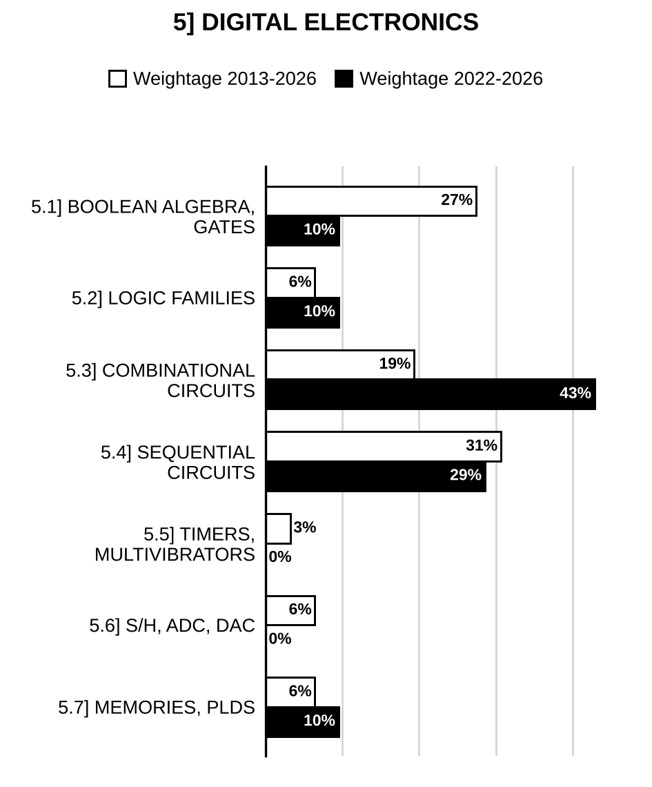
5.1] Boolean algebra and logic gates
23 questions
Consider the control circuitry of a machine copier with four switches as shown below in the figure. These switches are at various points along the path of the machine. Each switch is normally open and closes only when the paper passes over it. Let there be a restriction that switch 1 and switch 4 cannot close simultaneously. Use Karnaugh map to design a logic circuit that produces a high output whenever two or more switches are closed at the same time.
[Figure: Four switches SW1, SW2, SW3, SW4, each connected between a common grounded line and one input line of a block “Logic Circuit”; each input line is pulled up to 5 V through a resistor. The Logic Circuit has output X. Caption: (SW1, SW2, SW3, SW4: Switch 1, Switch 2, Switch 3, Switch 4)] [2023/20m/4b]
Consider the four variables logic function defined as follows: Assuming input variables as A, B, C and D, propose a logic circuit using only three logic gates to implement the function. [2021/10m/1e]
Design a combinational circuit to implement the minimal sum-of-products of the logic function . [2020/10m/2c]
Simplify the following expression using Boolean algebra: and draw the logic diagram for reduced expression. [2019/10m/5b]
Reduce the combinational logic circuit shown in Figure 7(d) to a minimum form.
[Figure: Figure 7(d): Inputs A, B and C each pass through an inverter; the three inverted signals feed a 3-input AND gate; the AND output passes through an inverter to a node; from the node, one path goes to a second AND gate (drawn with only this one input connected) whose output goes to an OR gate; a second path from the node goes directly to another input of the same OR gate; input D goes directly to the third input of the OR gate; the OR gate output is X] [2019/10m/7d]
Convert the following logic equation to NAND logic and draw the circuit using NAND gates: [2018/20m/2a]
For the Boolean function (i) find all the prime implicants; (ii) give minimal representation; (iii) find minimal two-level realization using NAND gates only. [2017/20m/2a]
Prove that . [2017/10m/5a]
Minimize the SOP terms given for a Boolean function Implement the minimized function using NAND gates alone. [2016/10m/5a]
Obtain all the possible minimal functions for: . [2015/10m/5e]
(i) Find 2’s complement of the following numbers: (1) 10010010 (2) 11011000 (ii) Convert the logical equation into product-of-sums (POS) form and design circuits using (1) OR and AND gates and (2) NOR gates. (iii) Explain the function of Schottky diode connected between the collector and base of transistors of TTL gate. [2014/20m/6b]
Determine the MSP form of the switching function using 6-variable Karnaugh map. [2013/20m/6a]
Assuming that logic 0 is available, show that the INCLUSION gate is a universal building block. [2013/10m/6c]
Convert decimal 65,535 to its hexadecimal and binary. [2012/12m/5b]
Convert decimal number 40 into binary and hexadecimal numbers. [2011/20m/6a]
Design a combinational logic circuit which produces an output equal to ‘1’ if the input variables have more 1’s in the sequence than 0’s. The output is zero otherwise. Design the circuit for three variable inputs. Draw the realization. [2009/10m/7a(i)]
Implement an OR gate with AND and NOT gates. [2007/5m/5b(ii)]
Minimize and implement the following multiple-output functions [2006/10m/6a(iii)]
A locker can be opened by A and B when they are both there, as the locker has 2 keys, one of which is with A and the other with B. C has both the keys, but he is permitted to open the locker only when B is not there. Show that the locker can be opened always if both A and C are there. Give the Boolean identity that symbolisms this situation. [2002/20m/3a]
A farmer (F) has two sheds ( & ) in his farm to keep his farm produce and belongings. He keeps vegetables (V) as farm produce, a goat (G) which can eat the vegetables and a dog (D) that can bite the goat in the absence of the farmer. The farmer along has to manage both sheds without loosing either vegetables or the goat. Suggest a logic circuit that can alarm him under any catastrophic condition by means of a buzzer. [2001/20m/1b]
Simplify the Boolean function and realise it using NAND gates. [1999/10m/5b(i)]
Reduce the following four variable function using Karnaugh map and implement it in NAND logic, [1998/20m/2c]
Minimize the following logic functions using Karnaugh maps and realize them using NAND gates. (i) (ii) [1997/20m/5a]
5.2] Digital IC families
10 questions
Draw the circuit diagram, function table, logic symbol and switch model for a CMOS gate (using six transistors) with two inputs and and an output , such that [2024/20m/2a]
(i) Find 2’s complement of the following numbers: (1) 10010010 (2) 11011000 (ii) Convert the logical equation into product-of-sums (POS) form and design circuits using (1) OR and AND gates and (2) NOR gates. (iii) Explain the function of Schottky diode connected between the collector and base of transistors of TTL gate. [2014/20m/6b]
Specify power supply voltage range, output logic 1 level voltage and output logic 0 level voltage for standard TTL gates. [2013/10m/5a]
Draw the circuit of TTL NAND gate and explain its operation. [2010/5m/1b(ii)]
The above circuit is intended for NOT operation for input levels 0 and 10 V. Calculate the minimum value of R for which this operation is possible. Assume , , in respect of above silicon transistor.
[Figure (printed before the text): NPN transistor inverter: input through a 10 kΩ resistor (current ) to the base node; from the base node a resistor R (current flowing down) to a −10 V supply; base current into the base; collector connected through a 2 kΩ resistor (current flowing down) to V; output taken at the collector; emitter grounded] [2007/10m/5b(i)]
Draw a positive logic OR gate with two diodes and explain its operation. [2007/5m/5b(iii)]
Describe what happens to each of the following CMOS characteristics as is increased (i) Noise margin (ii) Power dissipation (iii) Switching speed. [2006/5m/4a(iv)]
Draw the circuit diagram of a NOR gate using MOS transistors (n-channel) and verify the NOR operation with. The description of the functioning of this gate. [1997/15m/6a]
Show that the NMOS circuit of Fig. 5b is a NAND gate for positive logic. Write down the various combinations of inputs and output in a tabular form and clearly state the meanings of any symbols or parameters used therein.
[Figure: Fig. 5b: Two n-channel MOSFETs (upper, gate input ) and (lower, gate input ) in series between the output node and ground; load MOSFET (drawn horizontally, gate lead drawn upwards) between the output node and ; output taken from the node joining and the drain of ] [1996/20m/5b]
Explain what you understand by: (i) MMIC (ii) MOSFET (iii) NMOS Growth (iv) CMOS Development (v) RAM Device (vi) SRAM Cell (vii) DRAM Cell. [1996/20m/12c]
5.3] Combinational circuits
22 questions
A combinational logic circuit consisting of two numbers of 2 to 4 decoders is shown in the figure below: In this circuit, are the inputs and to are the outputs of the first decoder, while are the inputs and to are the outputs of the second decoder. Determine the logic expressions for and in terms of and .
[Figure: First “2 to 4 Decoder”: input → , input → ; outputs , , , ( and are left unconnected, ending in dots). and are each connected to both gates: an XOR gate with inputs (upper) and (lower), whose output drives ; and an XNOR gate (XOR with output bubble) with inputs (upper) and (lower), whose output drives . Second “2 to 4 Decoder”: inputs , ; outputs , , , ] [2026/10m/1d]
Consider the Boolean function: Implement it with a 4-to-1 multiplexer and external gates. Connect inputs A and B to the selection lines. Input to the four data lines is a function of the variables C and D which are obtained by expressing F as a function of C and D for each of the four cases when AB = 00, 01, 10 and 11. Functions are to be implemented with external gates. [2025/20m/3a]
A Binary Coded Decimal (BCD) code is to be transmitted to a remote receiver. Bits are arranged as . Design a circuit at the receiving end which has an error detector to check the legal BCD code and produce a HIGH for any error condition. [2024/10m/1d]
Find the logic equations for the outputs in the concise form and write the corresponding truth table for the circuit given below:
[Figure: Logic circuit with inputs and and four NAND gates. Gate G1: 2-input NAND with inputs and ; its output line N runs vertically. Gate G2: 2-input NAND with inputs and N; output . Gate G3: 2-input NAND with inputs N and ; output . Gate G4: 3-input NAND with inputs N, and ; output . Line N is also taken out directly as output .] [2024/10m/3c]
A circuit using three 2-input multiplexers is shown below. Determine the function performed by this circuit:
[Figure: Inside a dashed box: upper MUX with data inputs (top) and , output ; lower MUX with data inputs (top) and , output ; the select inputs S of both these MUXes are connected together to external input . A third MUX takes (upper input) and (lower input), its select S driven by external input ; its output is .] [2024/10m/4c]
Use multiplexer and logic gates to implement the function: [2023/10m/3a(ii)]
Explain the parity bit generator and parity bit checker. Realize the even parity bit generator and even parity bit checker using X-OR gate. [2022/10m/1e]
Draw the diagram of cascading BCD adders to add two three-digit decimal numbers. Also explain the function of this adder with suitable example. [2022/10m/8a(ii)]
(i) Verify by determining the logic equation for the output and by constructing the truth table for the logic circuit shown in Figure 4(b). (ii) Use an 8 to 1 multiplexer and logic gates to implement the following function:
[Figure: Figure 4(b): Four 2-to-1 multiplexers with data inputs (0) / (1), (0) / (1), (0) / (1) and (0) / (1); their select inputs are all connected to a common line . Their outputs feed a 4-to-1 multiplexer: the multiplexer to input 00, to 01, to 10 and to 11. The 4-to-1 multiplexer has select inputs , and output Y.] [2021/20m/4b]
Draw a block diagram to implement logic using a multiplexer. [2013/10m/5e]
Implement the following: (i) Half-adder using basic gates (ii) flip-flop using – flip-flop (iii) 2 to 4 decoder using 1×4 demultiplexers. [2011/15m/5a]
Design a binary to Gray code converter. [2010/10m/3a(ii)]
Realize a half-adder circuit using only NOR gates. [2009/15m/5b]
Design a 2-input, 3-output circuit which can be used as half adder or half subtractor by choosing output points. [2006/5m/1b(iv)]
Design a combinational circuit that accepts a three-bit number and generates an output binary number equal to the square of the input number. [2005/10m/1b(i)]
Implement the Boolean function with an multiplexer with A, B and D connected to selection lines , , , respectively. [2005/5m/3a(iii)]
Using multiplexers, implement a full adder circuit. [2003/10m/8a(i)]
Devise a 4-bit odd parity generator function using 3-level NOT-NOR-NOR logic. [2002/20m/7a]
.
(i) Draw the truth table of an octal-to-binary encoder with the condition that the output F = 1 when at least one of the inputs is a 1. The octal input with highest number has the highest priority. What is the condition of binary outputs and F output, if the inputs ? [2001/10m/3a(i)]
(ii) Design a combinational circuit using AND gates and half adders that can multiply two 2-bit numbers and to produce 4-bit number , , and . [2001/10m/3a(ii)]
.
(i) Design a combinational circuit having 3 inputs and 6 outputs with the condition that the output number is square of the input number. [2000/10m/5b(i)]
(ii) A computer uses RAM chips of capacity 1024 × 1. How many chips are required and how their address and data bus be connected to provide a memory capacity of 1024 bytes? How chips would be connected to provide memory of 16 K bytes? [2000/10m/5b(ii)]
It is desired to add two one-bit binary words and produce the result as Sum and Carry. Prepare a truth table, Karnaugh map and Boolean expressions to design a Half-Adder using minimum number of NAND gates. [1997/20m/5b]
Design a combinational logic circuit to generate the 2’s complement of a 2-bit number. You may use two full adders and other gates as required but keeping the number of other gates to a minimum. [1996/20m/8c]

Preparing for Prelims too?
Our UPSC Prelims Topic-wise PYQ eBook covers every Prelims question with detailed explanations, so you can see exactly where UPSC asks from.
View the BookDownload Free Sample5.4] Sequential circuits
27 questions
Design a MOD-6 synchronous DOWN counter using – flip-flops. [2026/20m/6a]
Design a sequential circuit with two D flip flops A and B and one input X. Let the state of the circuit remain the same for X = 0. However, when X = 1, the circuit goes through the state transitions from 00 to 10 to 11 to 01, back to 00 and then repeats. [2025/10m/1d]
Consider the shift register shown in the figure below, which is implemented using D flip-flops and multiplexers.
[Figure: Four D flip-flops 0, 1, 2, 3 (outputs , , , ), each fed at its D input by a 2:1 multiplexer. MUX 0: input 0 = , input 1 = . MUX 1: input 0 = , input 1 = . MUX 2: input 0 = , input 1 = . MUX 3: input 0 = , input 1 = . The select inputs of all four multiplexers are connected to the common Load line. The clock inputs of all flip-flops are connected to CK and their CLR inputs to the common line. Output taken from flip-flop 3.]
Complete the truth table shown as follows:
| CK (Inputs) | (Inputs) | Load (Inputs) | (Next State) | (Next State) | (Next State) | (Next State) |
| X | 0 | X | ||||
| ↑ (rising edge) | 1 | 0 | ||||
| ↑ (rising edge) | 1 | 1 |
Complete the timing diagram below assuming .
[Figure: Timing diagram: CK with 13 clock pulses, dotted vertical lines at the rising edges of pulses 2 to 12. high throughout, going low just after the 12th rising edge (low during the last pulse). Load: low, goes high during the first clock pulse and returns low after the 2nd rising edge (high only at the 2nd rising edge), then stays low. : low, high from between the 7th and 8th rising edges to between the 9th and 10th rising edges (high at the 8th and 9th rising edges), then low. Rows , , , left blank to be completed.] [2023/10m/3a(i)]
The diagram of Master-Slave S-R flip-flop and the waveform applied to the Master flip-flop is shown in Figure 5(a). Draw the waveform that appears at the output of Slave flip-flop.
[Figure: Figure 5(a), Master-Slave S-R flip-flop built from NAND gates: input S and clock C go to NAND gate ; C and input R go to NAND gate . The outputs of and drive a cross-coupled NAND latch (output ) and (output ), each latch gate also taking the other’s output. C is also taken (by a wire running along the bottom) to an inverter whose output is . and go to NAND gate ; and go to NAND gate . The outputs of and drive a cross-coupled NAND latch (output ) and (output ). Input waveform (versus t): CLK is a train of four positive pulses numbered 1, 2, 3, 4; dashed vertical lines mark the falling edges of pulses 1, 2 and 3. S is low until the falling edge of pulse 1, high from the falling edge of pulse 1 to the falling edge of pulse 2, and low thereafter. R is high until the falling edge of pulse 1, low from the falling edge of pulse 1 to the falling edge of pulse 2, high from the falling edge of pulse 2 to the falling edge of pulse 3, and low thereafter.] [2022/10m/5a]
Differentiate between the functions of Decade counter and BCD counter with example. [2022/10m/8a(i)]
Consider the circuit shown in Figure 2(c) below. Let inputs A, B and C be all initially LOW. Output Y is supposed to go HIGH only when A, B and C go HIGH in a certain sequence. Determine the sequence that will make Y go HIGH. Modify this circuit to use D-Flip-flops.
[Figure: Figure 2(c): Two J-K flip-flops. First flip-flop: J = A, CLK = B, K connected to ground, output X. Second flip-flop: J = X, CLK = C, K connected to ground, output Y. The active-low CLR inputs (bubbles) of both flip-flops are connected together to a Start line, shown as a negative-going (LOW) pulse.] [2021/10m/2c]
Design a synchronous sequential circuit with D-flip-flops for a state diagram shown in Figure 4(b).
[Figure: Figure 4(b): State diagram with states 000, 001, 010, 011, 100, 101, 110, 111 and transitions 000 → 001, 001 → 100, 100 → 111, 111 → 101, 101 → 000, 110 → 101, 010 → 000, 011 → 100] [2020/20m/4b]
Convert a D flip flop to function as an S-R flip flop. Draw the circuit. [2018/10m/5a]
Design a synchronous counter using D flip flop that counts in the following sequence: 6, 3, 5, 0, 2, 6, 3, 5, 0, 2, 6, … Draw the circuit. [2018/20m/7b]
Find the state transition diagram and realization using J-K flip-flops to count Mod 7 in the following sequence: 000, 001, 011, 100, 101, 111. [2017/20m/7b]
Divide by N counter is shown in the figure below. If initially , , , what is the value of N?
[Figure: Three JK flip-flops FF2, FF1, FF0 (left to right) with a common CLOCK to all inputs. Connections: , ; , ; , . Outputs and brought out on the right] [2015/20m/6b]
Design a circuit that gives the input-output relationship shown in Fig. 4.
[Figure: Fig. 4 – Timing diagram. Input: a train of five positive rectangular pulses numbered 1, 2, 3, 4, 5. Output: low throughout, goes high at the falling (trailing) edge of input pulse 4 and returns low at the falling edge of input pulse 5 (dashed lines mark these two edges); i.e. one output pulse lasting from the end of pulse 4 to the end of pulse 5.] [2014/10m/5e]
A sequential machine produces an output of 1 only when exactly two 0’s are followed by a 1 or exactly two 1’s are followed by a 0. Determine the reduced state table of the machine. [2013/20m/6b]
Show how a D flip-flop can be converted to SR flip-flop. [2012/12m/5a]
Indicate how many flip-flops are required to construct each of the following counters: (i) mod–3 (ii) mod 6 (iii) mod–9. [2012/20m/6a]
Implement the following: (i) Half-adder using basic gates (ii) flip-flop using – flip-flop (iii) 2 to 4 decoder using 1×4 demultiplexers. [2011/15m/5a]
Draw symbolic representation for +ve edge triggered clock input in a flip-flop and mark transition time by an arrow in clock input waveform for it. [2011/20m/6b]
Design a decade counter using JK FF’s (MOD-10 counter) and draw the timing diagrams. [2010/8m/2b(iii)]
Convert a clocked SR Flip-Flop to a clocked JK FF. [2010/10m/7a(ii)]
The figure below shows a divide-by- counter.
(i) Find . Assume initial value of , and . [2009/10m/2b(i)]
(ii) Repeat Part (i), if initially , and .
[Figure: Synchronous counter of three JK flip-flops (FF2, FF1, FF0 from left to right), the common Clock line connected to all three Ck inputs; , ; (crossing the vertical feedback line without connection); and also, from a junction dot on the line, fed back up and over the top to ; fed back along the bottom to ; unconnected] [2009/10m/2b(ii)]
The waveforms shown in the figure below are applied to– 1. positive edge-triggered SR flip-flop; 2. master-slave SR flip-flop. Draw the output waveforms in each case.
[Figure: Timing diagram. Clock: five positive pulses; the edges are labelled in order a (rising), b (falling), c (rising), d (falling), e (rising), f (falling), g (rising), h (falling), i (rising), j (falling). S: low at first, goes high shortly before a, goes low between b and c, high between d and e, low between f and g, high between g and h, low between h and i, and stays low to the end. R: low at first, goes high between b and c (at the same instant S goes low), low between c and d, high between f and g (at the same instant S goes low), low between g and h (at the same instant S goes high), high again between i and j and stays high to the end] [2009/10m/7a(ii)]
A partially filled truth table of a sequence generator (3-D flip-flops in cascade) is given below. Find the sequence generated. is LSB and is MSB.
| State | |||
| 1 | 1 | 0 | |
| 2 | 0 | ||
| 3 | |||
| 4 | 1 | ||
| 5 | 0 | 1 | |
| 6 | |||
| 7 | 1 | 1 | |
| 1 | 0 | 0 |
[2007/10m/1b(i)]
Draw the logic diagram and timing diagram of a 3-bit binary ripple up counter using positive edge triggered FF’s. [2006/5m/8a(iv)]
A sequential circuit has one input and one output. The state diagram is shown in the figure. Design the sequential circuit using D flip-flop.
[Figure: State diagram with five states 000, 001, 010, 011, 100; transitions labelled input/output: 001 → 001 on 0/0 (self-loop), 001 → 100 on 1/1; 100 → 011 on 1/0, 100 → 010 on 0/0; 011 → 001 on 0/0, 011 → 010 on 1/1; 010 → 010 on 0/0 (self-loop), 010 → 000 on 1/1 (printed “1/3”); 000 → 100 on 1/1; a line labelled 0/0 joins 011 and 000 (arrowhead direction unclear in the scan, probably 000 → 011) [?].] [2005/5m/6a(iii)]
The clock frequency of 1000 ns is connected to a 3-bit asynchronous counter with each flip-flip having 50 ns propagating delay. Which slate will never occur in it, if the clock frequency is decreased to 100 ns? Explain it by drawing wave- shapes for 1000 ns and 100 ns clock frequencies separately. [2000/20m/2a]
What is a race condition? How is it prevented? [1999/10m/5b(ii)]
The circuit shown in Fig. Q. 5(d) is using master-slave flip-flops. is high and can be taken to be 1. Find and for the first seven clock cycles after these are initially cleared. Give precise explanations for your answers.
[Figure: Fig. Q.5(d): Two JK master-slave flip-flops. FF1: inputs and tied together to ; clock input driven by CLK; output gives and also drives the clock input of FF2. FF2: inputs and tied together to terminal A (note: “A is at ”); output gives . The clear (CR) inputs of both flip-flops are joined and taken through a switch to ] [1995/20m/5d]
5.5] Comparators, timers and multivibrators
5 questions
Implement Astable Multivibrator using NAND gates and explain its operation. [2019/10m/6c]
A comparator and limiter circuit is shown in Fig. 2. Develop transfer characteristics vs. and explain.
[Figure: Fig. 2 – Op-amp inverting circuit: input through resistor to the inverting (–) input; non-inverting (+) input grounded. Feedback from the output to the inverting input through resistor , and in parallel with two Zener diodes connected back to back in series (cathode to cathode): Zener with its anode at the inverting-input side, and Zener with its anode at the output side.] [2014/10m/1d]
Using IC 555 and other suitable components, draw the circuit diagram of a missing pulse detector and explain its working. [2011/20m/4b]
Realize an Astable Multivibrator using 555 timer to produce a square wave of frequency 1 kHz with duty cycle of 50%. Mention three applications of timer. [2010/7m/5b(iii)]
Design an astable multivibrator with LM 555. Calculate also the duty cycle and frequency of oscillation. [1999/10m/2b(ii)]
5.6] Sample and hold circuits, ADCs and DACs
9 questions
Draw the block diagram of a single slope type A/D converter and explain its principle of operation. [2019/20m/8a]
Identify the circuit shown in Fig. 6(a). Briefly explain the same. Calculate the current and , if and :
[Figure: Fig. 6(a): R–2R resistor ladder feeding an op-amp: reference at the left node N0; series resistors from N0 to N1, from N1 to N2, from N2 to N3; from N3 a final resistor to ground carrying current (arrow from N3 towards this 2R). Shunt resistors: from N0 to ground; from N1 to the op-amp inverting-input line; from N2 to ground; from N3 to the op-amp inverting-input line. Op-amp: inverting (−) input joined to the lines from the N1 and N3 shunt resistors, feedback resistor from output to the inverting input, non-inverting (+) input grounded] [2016/20m/6a]
With the aid of circuit, draw ladder DAC and discuss its operation. [2010/6m/6b(ii)]
With for the DAC, find the resolution and full-scale output of this converter. [2010/4m/6b(iii)]
A D/A converter has the lowest and the highest values of resistances 1 kΩ and 4 kΩ, respectively. If the bit-length of the converter is to be increased by 2, what would be the number of resistors required and their values? Draw the complete circuit of the new converter. [2007/10m/1b(ii)]
Determine (1) maximum conversion rate (2) average conversion rate (3) maximum conversion time for a 16–bit counter type A/D converter using a 1 MHz clock. [2006/5m/5b(iv)]
Describe any two types of A to D converters. Discuss their merits and demerits. [1999/20m/6c]
For the R-2R type of digital-to-analog converter shown in Fig. 4c, find the output voltage when is closed and , and are grounded.
[Figure: Fig. 4c: R-2R ladder DAC. Reference battery = 15 V [?] (+ at top) between a top reference line and ground. Ladder line along the bottom: from ground a 2R resistor to node P, R from P to Q, R from Q to S, R from S to T. Four 2R legs hang from nodes P, Q, S and T respectively; the upper end of each leg goes to a changeover switch ( for P, for Q, for S, for T) that connects it either to the top reference line () or to ground. Node T feeds the non-inverting input of an op-amp connected as a voltage follower (output joined to the inverting input); output ] [1996/20m/4c]
Describe a successive approximation type of an A to D converter and give its merits. Find the conversion time and the resolution of an 8-bit ADC of this type when the clock period is 1.25 μs. [1995/20m/8c]
5.7] Memories and programmable logic
10 questions
Design a Programmable Logic Array (PLA) for a combinational logic circuit that computes the square of 3-bit binary numbers. Determine the minimum number of product terms required and construct the corresponding PLA programming table for the implementation. [2026/20m/7a]
Implement the following Boolean functions with a 4 × 3 Programmable Logic Array (PLA): ; ; [2020/10m/1e]
What is a PLA? Realize the following functions using an appropriate PLA: [2016/10m/7a]
What would be the binary address for a memory system having a capacity of bits. For the above memory system, what is the decimal address for the binary address 1011001101? What is the address in hexadecimal? [2012/20m/7a]
Write the full form of FPGA and explain why it is useful for prototyping of digital circuits. [2011/20m/6c]
Using a bipolar PROM, implement the following equations simultaneously: ; ; [2005/5m/7a(iii)]
It is desired to generate the following three Boolean functions ; ; By using an OR gate array as shown in Figure, where to are the product terms in one or more of the variables, and . Write down the terms , , , and .
[Figure: OR array with five horizontal product-term lines to (top to bottom) and three vertical output lines , , ; connections (dots) at: – and ; – and ; – and .] [2003/10m/8a(ii)]
.
(i) Design a combinational circuit having 3 inputs and 6 outputs with the condition that the output number is square of the input number. [2000/10m/5b(i)]
(ii) A computer uses RAM chips of capacity 1024 × 1. How many chips are required and how their address and data bus be connected to provide a memory capacity of 1024 bytes? How chips would be connected to provide memory of 16 K bytes? [2000/10m/5b(ii)]
Name the different types of Read- Only-Memories and briefly discuss their attributes in terms of programmability volatility, erasability, technology used and utility. [1997/20m/6b]
Explain what you understand by: (i) MMIC (ii) MOSFET (iii) NMOS Growth (iv) CMOS Development (v) RAM Device (vi) SRAM Cell (vii) DRAM Cell. [1996/20m/12c]

Strengthen your GS papers
Our UPSC Mains Topic-wise & Year-wise PYQ eBook (2013–2026) maps every GS question to the syllabus, so you know what UPSC asks and how often.
View the BookDownload Free Sample« Previous: Analog Electronics | Next: Energy Conversion »
Back to: Electrical Engineering Optional PYQs – Topic-wise
Last updated: 30 October 2026