
Here are all 144 Circuits—Theory questions asked in UPSC Electrical Engineering Optional Paper I from 1995 to 2026, arranged under the 8 topics of the official syllabus. Within each topic the latest questions come first.
Each question ends with a code such as [2024/15m/3b] – the year, the marks, the word limit (where UPSC set one) and the question number in the paper.
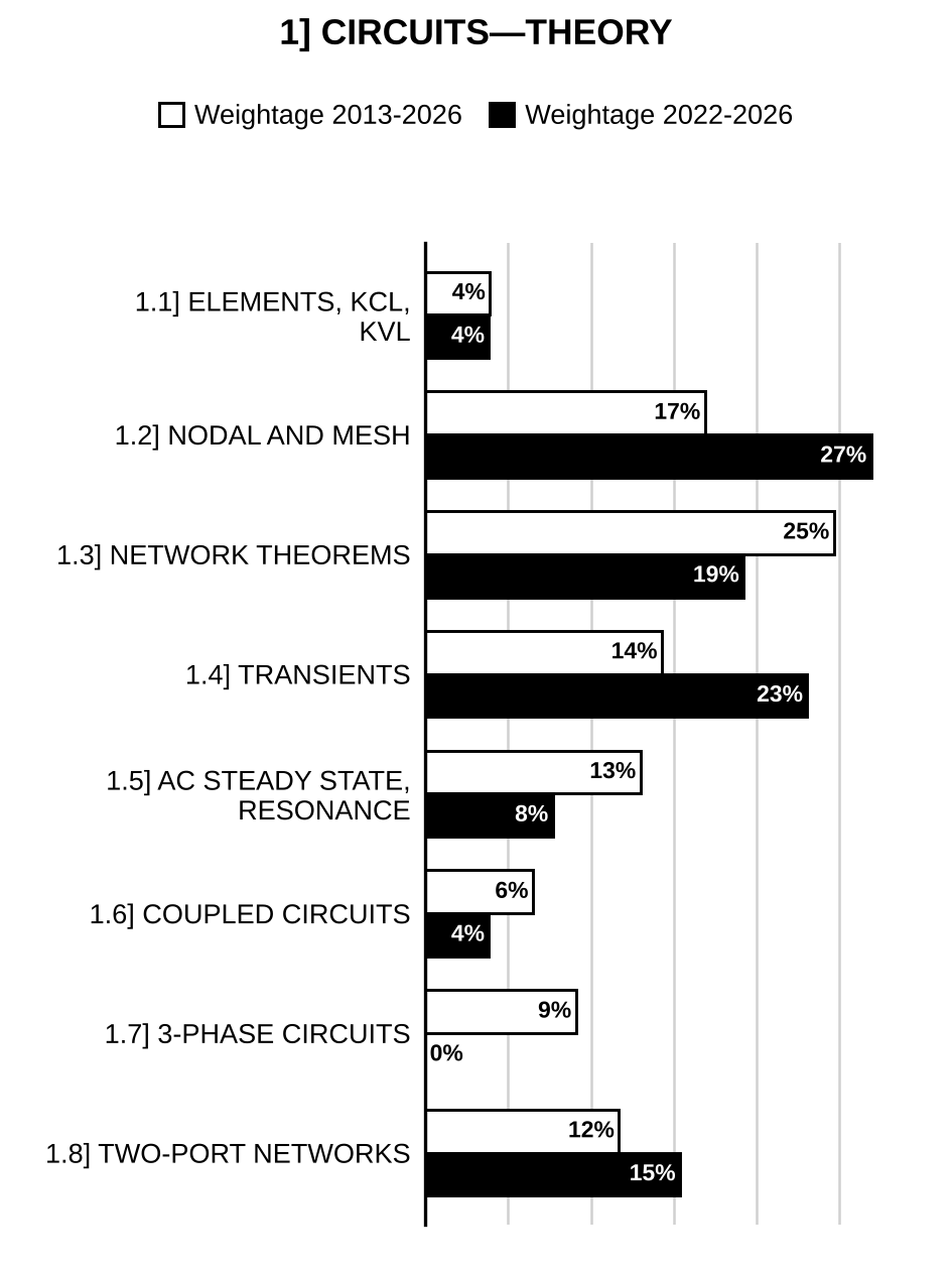
1.1] Circuit elements, network graphs, KCL and KVL
13 questions
For the circuit shown in Figure 1(a), find the , and power supplied by the dependent source.
[Figure: Figure 1(a): Circuit with a common bottom (return) wire. Left branch: independent voltage source , + terminal at top, connected between the bottom wire and the top-left node. Top-left wire carries current 2 A (arrow pointing right) through a 5 Ω resistor and then a 60 V independent voltage source (− terminal on the left, + terminal on the right) to the top middle node. Middle branch from the top middle node down to the bottom wire: current (arrow pointing down) through a 3 Ω resistor in series with a battery (− terminal on top, + terminal at the bottom). From the top middle node a 2 Ω resistor goes right to the top-right node; current 8 A is marked on this wire with the arrow pointing left (from the top-right node towards the 2 Ω resistor). Right branch from the top-right node down to the bottom wire: dependent (diamond) voltage source , + terminal at top.] [2022/10m/1a]
The reduced incidence matrix of an oriented graph is given as (i) Draw the graph. (ii) How many trees are possible for this graph? (iii) Write the tie-set matrix. [2016/10m/1a]
Find the values of and in the circuit shown in Fig. 1.
[Figure: Fig. 1 – Ladder network. Voltage source on the left (+ terminal at top) between the top rail and the bottom (return) rail; current flows from the + terminal of to the right through a series 2 Ω resistor along the top rail to node 1. From node 1 a 6 Ω resistor goes down to the bottom rail; a second series 2 Ω resistor goes along the top rail from node 1 to node 2. From node 2 a 4 Ω resistor goes down to the bottom rail carrying a marked current of 2 A (arrow pointing downward through the 4 Ω); a 2 Ω resistor from node 2 to the bottom rail is in parallel with the 4 Ω (rightmost branch).] [2014/10m/1a]
A storage battery has a no-load terminal voltage of 6 V. When the current through the battery is 100 A, the terminal voltage drops to 5 V. Show a pictorial representation of the battery as a constant current source. [2011/15m/1a]
The current is passed through a capacitor of 0.5 farad. Find the expression for the voltage across the capacitor in the time interval . [2009/5m/1a(i)]
For the circuit given below draw the network graph and draw any three possible trees of the network. Prove that for the network graph L = B − (N − 1) where L = no. of links B = no. of branches N = no. of nodes.
[Figure: Triangular network with an internal star: outer vertices T (top), BL (bottom left) and BR (bottom right) and a central node O; side T–BL: 10 Ω in series with a 10 V source (polarity marks not clearly legible); side T–BR: 10 Ω; side BL–BR: 10 Ω; 5 Ω from each of T, BL and BR to the central node O] [2006/5m/3a(i)]
Define the following terms related to electrical circuits An ideal filter SPICE Network graph d. [2006/5m/8a(i)]
For the circuit shown below, find , , and .
[Figure: Circuit drawn as a horizontal chain of elements between six nodes A–F from left to right: 25 Ω resistor from A to B, with voltage across it (+ at A); a dependent (diamond) current source from B to C, arrow pointing towards C; 10 Ω resistor from C to D; independent 25 A current source from D to E, arrow pointing towards D (leftwards); 100 Ω resistor from E to F. Four curved wires short pairs of nodes: an upper arc from A to C carrying current (arrow left to right), an upper arc from C to E carrying (arrow left to right), a lower arc from B to D carrying (arrow left to right) and a lower arc from D to F carrying (arrow left to right).] [2005/5m/1a(ii)]
What is cut-set in linear graph theory? Explain with an example. In the graph.
[Figure: Oriented graph with nodes ① (left), ② (middle of the top horizontal line), ⑤ (right) and ④ (bottom, also marked 0). Branches: 3 – upper arc from node 1 to node 5 (arrow towards 5); 2 – from node 1 to node 2 (arrow towards 2); 4 – from node 5 to node 2 (arrow towards 2); 6 – vertical, from node 2 down to node 4 (arrow downwards); 1 – between node 4 and node 1, arrow pointing towards node 1; 5 – between node 4 and node 5, arrow towards node 5 [?].]
check if the sets of branches {1, 3, 4, 6} {1, 2, 3}, {1, 2, 3, 5} constitute cut-sets. [2001/20m/7a]
A non-sinusoidal current i(t) as shown in the above figure is passed through a capacitance C = 100 μF. Determine the voltage across the capacitance when ω = 1000 rad/sec.
[Figure (printed above the text): Waveform of i(t) against θ = ωt: triangular wave starting at +I at θ = 0, falling linearly through zero at π/2 to −I at π, then rising linearly through zero at 3π/2 to +I at 2π.] [2000/20m/5a]
Determine the resistance across the terminals A and B of the network shown in the above figure.
[Figure: Twelve 10 Ω resistors forming the edges of a cube, drawn as two nested rhombuses: outer rhombus with corners L (left), T (top), B (right, terminal B) and D (bottom), edges L–T, T–B, L–D, D–B each 10 Ω; inner rhombus with corners A (left, terminal A), T′ (top), R′ (right) and D′ (bottom), edges A–T′, T′–R′, A–D′, D′–R′ each 10 Ω; four connecting resistors L–A, T–T′, R′–B and D–D′, each 10 Ω. Terminals A and B are diagonally opposite corners of the cube] [1999/20m/4c]
Fig. 1 (a) shows a network of resistors each of R ohms. Find the resistance between the terminals P and Q.
[Figure: Fig. 1 (a): Triangle of corners A (top), B (bottom left) and Q (bottom right) with a resistor R in each side (A–B, A–Q, B–Q); an inner node P inside the triangle connected to A through a vertical resistor R and to B through a resistor R; terminal P (small circle) is taken from the inner node and terminal Q (small circle) is joined by a wire to corner Q] [1997/20m/1a]
Fig. Q. 1(b) shows the details of a portion of a d.c. network. Evaluate the voltage V.
[Figure: Fig. Q 1(b): Two networks (top) and (bottom) joined by two vertical wires: in the left wire a current of 3 A flows downwards (from to ), in the right wire a current of 2 A flows upwards (from to ). A third terminal of is connected by the top line to the top corner of a bridge, and a third terminal of by the bottom line to the bottom corner of the bridge; the voltage between the top and bottom lines is marked [?] (+ at the top line). Bridge (diamond) arms: top corner to left corner 1 Ω; top corner to right corner 3 Ω; left corner to bottom corner 1 Ω; right corner to bottom corner 1 Ω [?]; between the left and right corners a 1 Ω [?] resistor in series with a 4 V battery (polarity not legible)] [1995/20m/1b]
1.2] Nodal and mesh analysis
15 questions
For the circuit shown below, if the power loss in resistor is 16 W, find the value of in the dependent source using nodal method:
[Figure: Circuit with a bottom reference (ground) rail. Left branch: 10 A independent current source, arrow pointing up, from the bottom rail to node . Node : resistor from down to the bottom rail, carrying current marked downward (from into the ). From to the right: resistor in series with a dependent (diamond) voltage source (− terminal on the side, + terminal on the side) to node . Node : resistor from to the bottom rail; 20 V independent voltage source from to the bottom rail, + terminal at the top ()] [2026/10m/1a]
For the circuit shown below, find the value of , if the power supplied by both the sources is equal:
[Figure: Ladder circuit with a common bottom rail. Left: 100 V independent voltage source, + terminal at top, from the bottom rail to the top-left node. resistor from the top-left node to node 1; resistor from node 1 to the bottom rail; resistor from node 1 to node 2; resistor from node 2 to the bottom rail; 10 A independent current source, arrow pointing up, from the bottom rail to node 2 (right-most branch)] [2026/10m/2a(ii)]
In the circuit given below, find the voltages at point A and point B.
[Figure: Triangular network with ground node G at the bottom. Top branch: A – – node N – – node R; a 3 A current source is connected between N and R in parallel with the (drawn above it, arrow pointing left, i.e. from R towards N); node R is joined to node B by a wire. Node A is wired directly to an inner node P, and node B is wired directly to an inner node Q; a resistor joins P and Q. A resistor from P and a resistor from Q meet at an inner node M, which is wired directly to G. Left outer branch: from A, a 6 V source (+ terminal towards A, − towards G) in series with a resistor down to G. Right outer branch: from B, a resistor in series with a 12 V source (− terminal towards B, + terminal towards G) down to G. G is grounded] [2025/10m/1a]
Find the voltage on points and of the given circuit:
[Figure: Circuit with a common bottom (ground) rail. Left: 10 V source (+ at top) from ground to the top-left node. 2 Ω from the top-left node to node A (current arrow marked at A pointing down). 2 Ω from node A to ground. 1 Ω from node A to a node P; a 2 A current source from P to node Q, arrow pointing right (towards Q). 5 V source (+ at top) from node Q to ground. From node Q the top wire continues to the right-hand branch: 2 Ω and 3 Ω in series from the top rail down to ground, with terminal B at their junction (2 Ω above B, 3 Ω below B).] [2024/10m/1a]
In the circuit given here, find the value of voltage :
[Figure: Two sub-circuits sharing a common bottom rail. Left part (its own top node): 12 mA current source (arrow up, into the top node); dependent current source (diamond, arrow up); 2 kΩ resistor carrying (+ at top); 2 mA current source (arrow down, from top node to bottom rail) — all four in parallel between the left top node and the bottom rail. Right part (separate top node M): 1 kΩ resistor with voltage (+ at top) from M to the bottom rail; current source −5 mA (arrow up) from the bottom rail into M; 4 kΩ from M to node X; 5 V voltage source (+ at top) from X to the bottom rail; from X a 1 kΩ resistor in series with a 2 mA current source (arrow up, towards X) down to the bottom rail.] [2024/10m/2c]
For the circuit shown in the figure, obtain the value of voltage across 0.5 Ω and 2.5 Ω resistors using nodal current analysis.
[Figure: Diamond-shaped network with outer nodes (top), (left), (right), (bottom) and a central node that is grounded (reference). Outer branches: 0.5 Ω between and , with voltage across it (+ at the end, − at the end); 2 Ω between and ; 2.5 Ω between and , with voltage across it (+ at the end, − at the end); dependent voltage source between and (+ at the end). Branches to the central (ground) node: 12 V source from (− terminal at , + terminal at the centre); 2 A current source from the centre to (arrow up towards ); 1 Ω from the centre to ; dependent current source from the centre to (arrow towards ). (In the scan the + signs of , and are printed like “×”.)] [2023/20m/2a]
Find the values of branch currents , and as indicated in the circuit of Figure 5(e).
[Figure: Figure 5(e): Current source (arrow upward) between the bottom wire and the top-left node; 10 Ω resistor from the top-left node to the bottom wire carrying downward; from the top-left node, 1 Ω resistor in series with (current flowing to the right) to the middle node; capacitor from the middle node to the bottom wire carrying downward; from the middle node a 5 Ω resistor (current to the right) to the + terminal of a dependent voltage source (+ at top) whose other terminal is on the bottom wire] [2020/10m/5e]
In the circuit shown in Figure 3(c), find the voltage across the 8 Ω resistor.
[Figure: Figure 3(c): Ladder circuit between a top rail and a common bottom rail. From left: 4 Ω resistor from top-left node to bottom; 3 A current source from the same top-left node to bottom, arrow pointing downwards (current flows from the top node down into the bottom rail); 2 Ω resistor in the top rail from the top-left node to the middle node; 8 Ω resistor from the middle node to bottom, voltage across it with + at the top (middle node) and − at the bottom; 3 Ω resistor in the top rail from the middle node to the right branch; right branch is a 12 V battery to the bottom rail, positive (long) plate at the top] [2018/10m/3c]
For the circuit shown in Fig. 2(a), find the value of , if the power dissipation in the load resistance is 36 watts:
[Figure: Fig. 2(a): Two sections sharing a common bottom (reference) rail and joined only through that rail. Left section: d.c. source (battery, longer plate/+ at top) from the bottom rail up to the top wire; a 5 Ω resistor in the top wire with voltage marked across it (+ on the source side, − on the far side); beyond it a 2 Ω resistor and a 4 Ω resistor, each connected from the top wire to the bottom rail (in parallel). Right section: dependent current source (arrow pointing up) from the bottom rail to node P at the top; 10 Ω resistor in the top wire from P to node Q; 2 Ω resistor from Q to the bottom rail; 5 Ω resistor in the top wire from Q to node S; load from S to the bottom rail] [2016/20m/2a]
Determine the current in Fig. 4 using the ladder method.
[Figure: Fig. 4 – Ladder network. Source = 10 V (arrow up, + at top) on the left; top wire from the source through 2 Ω to node ; bottom wire from the source directly to node . 200 Ω between and . Top series 1 Ω from to ; bottom series 1 Ω from to . 50 Ω between and . Top series 2 Ω from to ; bottom wire to (no element). 100 Ω between and . From a series 1 Ω along the top, then down through 10 Ω (current downward) to the bottom wire at .] [2013/20m/2b]
Write the node equations for the network shown in Fig. 11. Assume node ② as a reference node:
[Figure: Fig. 11 – Nodes ① and ② on the top line and node ③ the bottom line. Left: source (+ at top) from node ③ through a 5 Ω resistor to node ①; inductor from node ① to node ③; 4 Ω resistor between nodes ① and ②; capacitor from node ② to node ③; 2 Ω resistor from node ② to the + terminal of source , whose other terminal goes to node ③] [2010/10m/8a(ii)]
For the circuit shown below, determine the numerical value of , using nodal analysis.
[Figure: Ground at the bottom line. Node A (top left): connected to ground through 0.5 Ω in series with a 2 V source (+ towards node A). Current flows from node A to node B through 1 Ω. Node B: 0.5 Ω to ground, and a 1 A current source from ground into node B (arrow upwards). Node B to node C through 1 Ω. Node A to node C directly through 2 Ω (top wire). Node C: 1 Ω to ground, and a 2 V source to ground (+ towards node C)] [2009/12m/4a(i)]
Determine the power delivered by 6 A source.
[Figure: Bridge network between a left node and a right node: upper branch 1 Ω (left) and 2 Ω (right) in series, meeting at an upper middle node; lower branch 4 Ω (left) and 3 Ω (right) in series, meeting at a lower middle node; a 5 V source connected between the upper middle node (+) and the lower middle node (−); an outer loop connects the left node and the right node through a current source marked 6 A (drawn in the bottom wire, arrow pointing right, i.e. towards the right node)] [2007/10m/1a(i)]
For the circuit shown in the figure determine using nodal analysis.
[Figure: All elements between a top wire and a common bottom wire: (from left) independent current source (arrow up), resistor , resistor connected at node V (current flowing down through ); resistor in the top wire from node V to the output node ; at the output node a dependent current source (arrow down) and resistor to the bottom wire; output terminal . , ] [2007/10m/1a(ii)]
For the network shown below, Find the current ratio transfer function given by .
[Figure: Ladder network between a common bottom (ground) wire and a top wire, from left to right: current source (arrow up) feeding the top wire with current (arrow to the right); 1 Ω shunt resistor to ground; series dependent voltage source (diamond, − on the left, + on the right) in the top wire; 1 Ω shunt resistor to ground carrying current (arrow upwards); series 2 Ω resistor in the top wire; shunt dependent current source (diamond, arrow upwards) labelled [?]; current flowing leftwards in the top wire from the right end into this node; 1 Ω shunt resistor to ground at the right end.] [2005/10m/4a(i)]
1.3] Network theorems
30 questions
In the circuit shown below, is the ac voltage source given by , with and . Calculate the value of load resistance for maximum power transfer and also find out maximum power transferred to load.
[Figure: Primary loop: ac source ( rad/sec.) in series with ohms and the primary winding of an ideal-coupled transformer; secondary winding connected across load . Dot marks at the top of both windings. Transformer data: , (Turns Ratio)] [2025/10m/4c]
In the circuit diagram given here, load resistance is to be set for maximum power transfer. Draw Thevenin equivalent circuit across and calculate the value of for maximum power transfer. Also calculate the power loss in resistance , when the circuit is delivering maximum power to load :
[Figure: 9 V source (+ at top) on the left between the bottom rail (b side) and the top-left node; from the top-left node to node P; from P down to the bottom rail: in series with a 3 V source (+ at top, towards ). From P a dependent voltage source (diamond, − on the left/P side, + on the right) to node a. from node a to the bottom rail (node b); variable load resistor across a–b; marked between terminals a and b.] [2024/20m/4a]
Obtain Norton equivalent circuit at terminals ab of the coupled circuit shown in the figure. Using it, find out the current passing through 5 Ω resistor connected between the terminals ab.
[Figure: Left source V (+ at top) and right source V (+ at top), both returning to a common bottom wire. From the top of the left source: 4 Ω in series with coil to the middle node, which is brought out as terminal a; from the middle node: coil in series with 2 Ω to the top of the right source. Terminal b is taken from the bottom wire. The two coils are magnetically coupled with mutual reactance ; dot on the coil at its left (4 Ω) end and dot on the coil at its right (2 Ω) end.] [2023/10m/1a]
Obtain the Thevenin’s equivalent of the network shown in Figure 2(a)(ii), across the terminals XY.
[Figure: Figure 2(a)(ii): A 4 V source (+ terminal on top) on the left, its top connected through a 2 kΩ resistor to a middle top node; from the middle top node a 3 kΩ resistor goes to terminal X. A dependent current source (diamond, arrow pointing up) is connected from the bottom wire up to the middle top node. The bottom wire joins the − terminal of the 4 V source, the dependent source and terminal Y. is the voltage across the terminals, + at X and − at Y.] [2022/10m/2a(ii)]
Using the superposition theorem find the voltage ‘V’ across the 5 Ω resistance in the circuit as shown in Figure 6(c).
[Figure: Figure 6(c): Four parallel branches between a top wire and a bottom wire, from left to right: a 2 A current source (arrow pointing up, i.e. current delivered into the top-left node); a 5 Ω resistor with voltage V across it, + at the top; then the top-left node connects through a 10 Ω resistor (in the top wire) to the top-right node; a 2 Ω resistor from the top-right node to the bottom wire; a 4 A current source (arrow pointing up) from the bottom wire to the top-right node. The bottom wire is common to all branches.] [2022/10m/6c]
Find the Thevenin’s equivalent of the circuit shown in Figure 2(a) below as seen from the load impedance . Also find the value of for maximum power transfer.
[Figure: Figure 2(a): Source on the left. From its top terminal a capacitor goes right to the dotted top end of coil ; coil runs down to a middle node. A second coil runs from the middle node up to its dotted top end, which connects through a inductor along the top wire to the right and down through the load to the bottom wire. The two coils are magnetically coupled with (dots at both top ends). From the middle node, 2 Ω in series with goes down to the bottom wire, which returns to the source.] [2021/20m/2a]
For the circuit shown in Figure 3(b), calculate the voltage as function of time, where and .
[Figure: Figure 3(b): AC source on the left; from its top a 10 Ω resistor to node . A 0.1 F capacitor from node to the bottom wire, voltage across it (+ at top). Node is joined along the top wire to a current source connected from the bottom wire up to the top wire (arrow pointing up). From there a 4 H inductor goes right to the + terminal of a 20 V dc source, whose − terminal is on the bottom wire. The bottom wire is common.] [2021/20m/3b]
An electrical network is fed by two ac sources, as shown in Figure 3(b)(ii). Given that , and . Find the values of Thevenin voltage and impedance across terminals X and Y.
[Figure: Figure 3(b)(ii): Source (+ at top) in series with to node X; source (+ at top) in series with to node X; connected between node X and node Y; node Y is the common bottom wire joining the lower terminals of both sources] [2020/10m/3b(ii)]
In the network shown in Figure 1(a), determine the following: (i) The value of the load resistance to have maximum power transfer (ii) The maximum power delivered to the load.
[Figure: Figure 1(a): 5 V dc source (+ at top) in series with to a middle node; from the middle node to the bottom wire; from the middle node to terminal a; variable load resistor connected between terminals a and b; terminal b on the bottom wire, which returns to the − terminal of the source] [2019/10m/1a]
Using Thevenin’s theorem, find the current through the 40 Ω resistor connected between terminals a and b in Figure 5(e).
[Figure: Figure 5(e): Bridge circuit fed by a 220 V battery in the left branch (long/positive plate at the top). Battery positive terminal connects through the top rail to two resistors: 3 kΩ from the top rail down to node a, and 400 Ω from the top rail down to node b. 1 kΩ from node a down to the bottom rail; 600 Ω from node b down to the bottom rail; bottom rail returns to the battery negative terminal. 40 Ω resistor connected between terminals a and b] [2018/10m/5e]
For the circuit shown in Fig. 1(a), find the current through 5 Ω resistor by using Thevenin’s theorem and verify the same by using superposition theorem.
[Figure: Fig. 1(a): Two sub-networks joined by two links. Left sub-network between node A (top) and node D (bottom), three branches in parallel: V battery (+ at top); a 20 Ω resistor; V battery (+ at top) in series with a 6 Ω resistor. Right sub-network between node B (top) and node C (bottom), three branches in parallel: V battery (+ marked at its lower terminal) in series with a 7 Ω resistor below it; V battery (+ at top); V battery (+ marked at its lower terminal) in series with a 4 Ω resistor below it. A 5 Ω resistor connects A to B (top link). Bottom link from D to C: battery V (+ on the side towards D) in series with a 10 Ω resistor] [2017/10m/1a]
In the network shown in Figure, determine the value of current through 1 Ω resistance connected between terminals A and B. Verify the answer using superposition theorem also.
[Figure: 4 V source (+ at top) on the left between the top wire and the bottom wire; 2 Ω resistor in the top wire from the source to the middle node; a 2 A current source (arrow pointing up) from the bottom wire to the middle node; 3 Ω resistor in the top wire from the middle node to terminal A; 1 Ω resistor between terminal A and terminal B, B being on the bottom wire] [2015/20m/4b]
Obtain the Norton’s equivalent circuit at the terminals and for the network shown in Fig. 3.
[Figure: Fig. 3 – Network with top rail and bottom rail (bottom rail ends at terminal B). Leftmost branch: 1 Ω resistor in series with a 100 V source (+ terminal toward the 1 Ω, i.e. upper end), connected between top-left node P and the bottom rail. Middle branch: 10 Ω resistor from node P to the bottom rail. From node P along the top rail: a 20 V source (– terminal at the P side, + terminal to the right) in series with a 2 Ω resistor to node Q, which connects to terminal A. Right branch: 10 Ω resistor from node Q to the bottom rail (B).] [2014/20m/4b]
Using -Y substitution, determine the resistance between and , in Fig. 1.
[Figure: Fig. 1 – Bridge (diamond) network with nodes (top), (left), (right), (bottom): 2 Ω between and ; 2 Ω between and ; 1 Ω between and (horizontal diagonal); 2 Ω between and ; 1 Ω between and .] [2013/10m/1a]
Consider the unbalanced Wheatstone bridge shown in Fig. 3: The internal resistance of the galvanometer is 1 ohm. Using Thevenin’s theorem, determine the galvanometer current.
[Figure: Fig. 3 – Wheatstone bridge with nodes (left), (top), (right), (bottom): 100 Ω between and ; 110 Ω between and ; 100 Ω between and ; 90 Ω between and ; galvanometer G between and . Source = 10 V (arrow pointing up, i.e. + toward the top) connected by the outer wires between (top) and (bottom).] [2013/20m/2a]
(i) Find Y and Z parameters for the following circuit: (ii) State Tellegen’s theorem for network analysis.
[Figure: Two-port: from the upper port-1 terminal (+, current entering) a current-controlled voltage source (diamond, + on the port-1 side, − on the right) in series to a node X; node X is connected directly (short circuit) to the lower common wire (node shown by a small circle); from node X a 2 Ω resistor to the upper port-2 terminal (+, current entering); across port 1, across port 2; the lower wire is common to both ports] [2012/20m/3a]
Using Millman’s theorem, find the current in the 10-ohm resistor in Fig. 2 (a).
[Figure: Fig. 2 (a): Ladder network with a common bottom (return) wire. Left branch: voltage source = 24 V (arrow upwards). From the top of a 2 Ω resistor to node P. Branch from P to the bottom wire: voltage source = 20 V (arrow upwards) in series with a 2 Ω resistor. From P a 2 Ω resistor to node Q; a 9 Ω resistor from Q to the bottom wire. From Q a 1 Ω resistor to node R; the 10 Ω resistor from R to the bottom wire, carrying current (downwards)] [2011/20m/2a]
State and prove maximum power transfer theorem. [2011/20m/2b]
Use Thevenin’s theorem to find the current in 4 Ω branch of the network given in Fig. 4:
[Figure: Fig. 4 – Left: 12 V source (+ at top) with current flowing from its + terminal through a 5 Ω resistor to node X; 12 A current source from the bottom (reference) line up into node X; from node X a current-controlled voltage source (diamond, + on the node-X side, − on the right) in series with the 4 Ω resistor, then a 1 Ω resistor, then a 20 V source (+ at top, − to the bottom line); the bottom line joins all the negative terminals] [2010/10m/2a(i)]
For the network shown below, determine which will receive maximum power.
[Figure: Left: 15 V source (+ at top) with current flowing from its + terminal through a 5 Ω resistor to node X; 10 A current source from the bottom line up into node X; from node X a current-controlled voltage source (diamond, + on the node-X side, − on the right) in series with the load (between two terminals), then a 1 Ω resistor and a 10 V source (+ at top, − to the bottom line); the bottom line joins all the negative terminals] [2009/8m/6a(ii)]
Use Thevenin’s theorem to replace the three-loop circuits of figure by a single-loop equivalent circuit in which the identity of is preserved. [2007/10m/6a(i)]
Find the value of so that the maximum power is consumed in it.
[Figure: Three-loop ladder with a common bottom wire: on the left a 60 V battery (+ at top) between the bottom wire and the top-left corner; top wire: 60 Ω from the top-left corner to node A; 30 Ω from node A to the bottom wire; from node A along the top wire a 50 V battery (+ terminal towards the right) in series with to node B; 60 Ω from node B to the bottom wire; from node B a 40 Ω resistor in the top wire to the top-right corner; a 100 V battery (+ at top) between the top-right corner and the bottom wire] [2007/10m/6a(ii)]
State and explain Thevenin’s theorem and replace the active network of the figure given below, at terminals ab with a Thevenin’s equivalent.
[Figure: Voltage source V = (+ at top) on the left; from its + terminal a 5 Ω resistor in the top wire to node X; from node X to the bottom wire a 3 Ω [?] resistor in series with an inductive reactance j4 Ω; from node X an inductive reactance j5 Ω in the top wire to terminal a; terminal b on the bottom wire, which returns to the − terminal of the source] [2006/10m/1a(i)]
If an impedance is connected across a voltage source V with source impedance , then for maximum power transfer, what will be the load impedance? [2004/4m/1a(ii)]
Determine the current in the 5 ohm resistor using Thevenin’s theorem.
[Figure: Ladder circuit: 50 V d.c. source on the left (+ at top) between the top wire and the bottom (return) wire; 1 Ω resistor in the top wire from the source to node 1; 5 Ω resistor from node 1 to the bottom wire; 1 Ω resistor in the top wire from node 1 to node 2; 1 Ω resistor from node 2 to the bottom wire; on the far right a current source of 8 A [?] (arrow pointing up, i.e. driving current from the bottom wire into node 2) connected between the bottom wire and node 2, in parallel with the last 1 Ω resistor] [1999/20m/1b]
Find X and; [?] in terms of R and R2 to give maximum power dissipation in R2 shown in the figure.
[Figure: a.c. source in series with resistor ; then a shunt reactance (inductor) across the line; then a series reactance followed by the load resistor across the line] [1998/20m/5b]
Calculate the power fed to the 15 Ω resistor by using Thevenin’s equivalent circuit for the portion to the left of points A and B in the circuit of Fig. 2 (b).
[Figure: Fig. 2 (b): Left loop: 100 V source (+ at top); 6.8 Ω resistor in the top line (voltage marked across it); then a 4 Ω resistor and an 18 Ω [?] resistor each connected from the top line to the bottom line. Right part (not wired to the left part): a dependent current source (arrow upwards) from the bottom line to the top line; 4.8 Ω in the top line; a 10 Ω resistor from the top line to the bottom line; 10 Ω in the top line to terminal A; 15 Ω resistor between A and B; 6 Ω in the bottom line from B back to the bottom line of the source] [1997/20m/2b]
Using Thevenin’s theorem, determine the current in the 2 Ω resistor in the circuit of Fig. 1c.
[Figure: Fig. 1c: Four parallel branches between a top line and a bottom (common) line. Branch 1 (left): voltage source 24 V [?] (+ at top) in series with an 8 Ω [?] resistor in the top line, the resistor joining the source to the top line node of branch 2. Branch 2: current source 2 A (arrow upwards) in parallel with a 20 Ω resistor, connected between the top and bottom lines. Branch 3: 10 Ω resistor in series with a battery of 36 V [?] (label blurred; plate polarity not legible), from the top line to the bottom line. Branch 4 (right): 2 Ω resistor between terminals A (top) and B (bottom), connected across the top and bottom lines] [1996/20m/1c]
Show that an n-mesh, passive, three-terminal network may be replaced by a delta-connection of three impedances. Here n can be arbitrarily large. [1996/20m/2b]
The two figures show a linear reciprocal 2-port network N under two different terminal conditions. The switches are closed at in both the circuits with zero initial conditions in N. Given that the currents in (i) for are: amps; amps, find for in (ii).
[Figure: Fig. Q2(b): (i) A 1 V battery connected through a switch (closed at t = 0) to port 1 (terminals 1–1′) of network N, input current entering terminal 1; port 2 (terminals 2–2′) short-circuited, with current in the short (arrow downwards from 2 towards 2′). (ii) Port 1 (1–1′) open-circuited, voltage across it (+ at terminal 1); a 2 V battery connected through a switch (closed at t = 0) across port 2 (2–2′)] [1995/20m/2b]
1.4] Transient analysis
20 questions
For the circuit shown below, steady state is achieved with switch open. At , switch is closed. Find the time expression of current in . Also find its initial and final values:
[Figure: 50 V voltage source (+ at top) on the left between the bottom rail and the top-left node; resistor in the top wire from the top-left node to node P; from node P to the bottom rail a resistor in series with a 1 H inductor; from node P along the top wire, switch (closes at ) to the top of , whose lower end is on the bottom rail] [2026/10m/3a(i)]
In the circuit shown in the diagram, initially key is closed and capacitor has no charge (at time ). Now at time seconds, key is opened and at seconds it is again closed. Plot output voltage across the capacitor with respect to time and find output voltage values at time 10 seconds, 18.68 seconds and 28.68 seconds.
[Figure: Bottom rail = terminal A (grounded). Node M (middle) and top node T. Between M and T: resistor (left) and, in parallel, a 1 A current source (arrow up, from M towards T). Between the bottom rail and M: key (left) and, in parallel, a 0.1 A current source (arrow up, from the bottom rail towards M). From T along the top: resistor, then a 5 V source (− on the left, + on the right) to node B (output terminal B). Capacitor from B to the bottom rail; OUTPUT taken between B and A] [2025/20m/2a]
In the circuit given here, is an ideal diode and key is ON for a long period of time. Now at time , key is opened. Draw the voltage waveform on capacitor and find the final steady-state voltage on the capacitor:
[Figure: 9 V source (+ at top) on the left; from its + terminal, inductor along the top to node N. From node N down to the bottom rail: key (marked “Open at ”) in series with . From node N the top wire continues through diode (anode at N, cathode to the right) to the top of capacitor , whose lower plate goes to the bottom rail, which returns to the − terminal of the 9 V source.] [2024/10m/1e]
In the series RLC circuit shown in the figure, the capacitor has an initial charge and the switch is in position 1 long enough to establish the steady state. Find the transient current which results when the switch is moved from position 1 to 2 at .
[Figure: The switch pole is connected along the top wire (current , arrow to the right) through 5 Ω and 0.1 H in series down to the bottom wire. Position 1 connects the pole to a 10 V source (+ at top) whose − terminal is on the bottom wire; position 2 connects it to a 200 μF capacitor carrying initial charge (− on the upper plate, + on the lower plate) whose lower plate is on the bottom wire.] [2023/10m/5e]
For the circuit shown in Figure 2(a)(i), initial current through the coil is zero. The switch is closed at time . Find the time domain expression of current flowing through the coil for . How long will it take for the coil current to reach 95% of its final value and what is the final value of this current?
[Figure: Figure 2(a)(i): Left branch: 100 V source (+ terminal on top) in series with a 50 Ω resistor above it; the top of the 50 Ω resistor connects through switch S (closes at ) along the top wire to the right. Middle branch: 100 Ω resistor from the top wire to the bottom wire. Right branch: 4 H coil from the top wire to the bottom wire, coil current marked by an arrow pointing down. The bottom wire joins the − terminal of the source, the 100 Ω resistor and the coil.] [2022/10m/2a(i)]
For the circuit shown in Figure 5(e), and . Calculate the value of for .
[Figure: Figure 5(e): Three branches between a top wire and a common bottom wire. Left branch: capacitor with voltage (+ at top). Middle branch: dependent current source (arrow pointing up). From the top of the middle branch a 3 Ω resistor runs along the top wire to the right branch. Right branch: capacitor , with current i in this branch marked by an arrow pointing up (towards the 3 Ω resistor).] [2021/10m/5e]
The switch shown in Figure 1(a) has been closed for a very long time and it is opened at time t = 0. (i) Find the value of for . (ii) Just after the switch is opened, find the value of . (iii) Determine the expression for for and find the value of .
[Figure: Figure 1(a): Three-branch circuit between a top wire and a bottom wire. Left branch: 100 V dc source, + terminal at top, connected through a 20 Ω resistor (in the top wire) to the top middle node. Middle branch (from the top middle node to the bottom wire): switch (opens at t = 0), 5 Ω resistor and a 100 V dc source in series, the source’s − terminal towards the 5 Ω resistor (top) and + terminal at the bottom wire. Right branch: 0.5 H inductor from the top wire to the bottom wire, current flowing downward through it] [2020/10m/1a]
Determine current i(t) in the circuit of Figure 5(d), for all values of time.
[Figure: Figure 5(d): Left branch: 100 V dc source (+ at top) between the bottom wire and the top-left corner; top wire: a voltage source (− on the left, + on the right) in series with a 5 Ω resistor to the top-right node; from the top-right node to the bottom wire two parallel branches: a 5 Ω resistor and a 10 H inductor carrying i(t) downward] [2019/10m/5d]
Consider the R-L-C circuit shown in Fig. 3(c), wherein Determine , and after the switch is closed.
[Figure: Fig. 3(c): Current source (arrow pointing upwards) in the left branch; a switch in the top wire closes at , connecting the source to three parallel branches: resistor R (current downwards), inductor L (current downwards) and capacitor C (current downwards); voltage across the parallel combination marked on the right by a double-headed arrow spanning the top and bottom wires (no polarity marked)] [2017/10m/3c]
In Fig. 5, capacitor is initially charged at 100 V and the other two capacitors are initially uncharged. The switch is closed at time . Find the current flowing through the resistor as a function of time.
[Figure: Fig. 5 – = 1 μF (left), = 1 μF (middle) and = 2 μF (right), each between the top wire and a common bottom wire. Switch in the top wire between and ; resistor = 500 Ω in the top wire between and .] [2013/10m/2c]
The switch is closed at in Fig. 2 (c). Using Laplace transforms, find , and the voltage across the inductance.
[Figure: Fig. 2 (c): 12 V battery (current leaving its upper terminal) in series with switch S and a 2 Ω resistor to node N; a 2 Ω resistor from N to the bottom (return) wire; from N a second branch carrying through a 2 Ω resistor in series with a H inductor to the bottom wire, which returns to the battery] [2011/20m/2c]
Determine the time constant for the network shown in Fig. 1:
[Figure: Fig. 1 – 10 V battery in series with switch S and resistor R; beyond R the circuit splits into two parallel branches, resistor 2R and capacitor C, each connected back to the other terminal of the battery] [2010/5m/1a(i)]
In the circuit shown below (Fig. 8), the switch is in position ‘1’ long enough to establish steady-state conditions and at is switched to position ‘2’. Draw ‘s-domain’ network:
[Figure: Fig. 8 – Switch S at the top left has its common terminal connected along the top line to a 25 Ω resistor in series with a 2 H inductor down the right side to the bottom line; position 1 connects to a 50 V battery (long plate, i.e. + terminal, towards the switch) whose other end goes to the bottom line; position 2 connects to a 100 V battery (drawn with the long plate, i.e. + terminal, towards the bottom line) whose other end goes to the bottom line; switch shown at position 1 with an arrow indicating movement to position 2] [2010/5m/5a(iii)]
Determine the currents , and at for the circuit given below. Assume that the voltage source is applied at .
[Figure: d.c. source (battery) on the left; current flows from its upper terminal through in the top wire to node P; from node P a vertical branch: (current flowing down) to node Q, then inductor L (current flowing down) from node Q to the bottom wire; from node P along the top wire to the right-hand vertical branch: capacitor from the top wire to node S and capacitor from node S to the bottom wire; a switch marked t = 0 connected between node Q and node S; the bottom wire returns to the lower terminal of ] [2006/10m/1a(ii)]
Find , , and for the circuit shown below. Use to denote . Assume the switch 1 has been opened for switch 2 has been closed for along time and steady-state condition prevails at .
[Figure: 10 V source (+ at top) in the left vertical branch; from its top terminal a 1 Ω resistor in series with Switch 1 (operated at t = 0) leads to node X; capacitor , ½ F (+ at top) from X to the bottom (ground) wire; a second 1 Ω resistor from X to node Y; 1 H inductor from Y to ground carrying (arrow downwards); a separate upper branch from X to Y consists of a 2 A current source (arrow pointing right, towards Y) in series with Switch 2 (operated at t = 0). The bottom wire is common to the source, capacitor and inductor.] [2005/6m/2a(i)]
Find the current i(t) through the 8 Ω resistor of the circuit diagram shown below with initial current Amp.
[Figure: Single series loop: voltage source 6u(t) (+ at top, arrow upwards) on the left; inductor L = 4 H in the top wire; resistor R = 8 Ω on the right side; bottom wire returns to the source; loop current i(t) clockwise.] [2004/6m/2a(ii)]
Circuit diagram shown below is initially under steady-state condition, the switch is moved from position 1 to position 2 at t = 0. Find the current after switching.
[Figure: 10 V battery on the left, its positive terminal connected by the top wire to switch contact 1; the switch blade is connected (common terminal) to one end of resistor (value illegible under the watermark) [?]; the other end of goes to the top of inductor L = 5 H, whose bottom goes to the bottom wire; switch contact 2 is connected through resistor (value illegible under the watermark) [?] to the bottom wire, which also returns to the battery negative terminal; the switch moves from 1 to 2 at t = 0; current i(t) marked clockwise in the loop –L–.] [2004/8m/5a(i)]
In the circuit shown below the switch ‘S’ closes at t = 0, and open after 10 ms. What will be the currents in and and , and voltage across 8 ms after switch ‘S’ opens? Assume to be an ideal diode and a 0.7 V drop across whenever it conducts.
[Figure: 200 V battery in the left vertical branch; from its top terminal the switch S, then inductor H in the top wire, with diode (unlabelled in the figure) connected in parallel across (its cathode towards the switch side, anode towards the right); the top wire continues to the right and down through to node N; from N, inductor H down to the bottom wire; also from N, a branch of capacitor in series with diode down to the bottom wire ( anode at the bottom wire, cathode towards ); the bottom wire returns to the battery.] [2003/20m/4a]
In the circuit of Fig 2 (c), when the switch is closed , it is noticed that mA and , sec. Assuming zero initial current for inductor and zero initial charge for capacitor, find the values of and and L.
[Figure: Fig. 2 (c): 5 V battery with a switch in the top line feeding two parallel branches: left branch in series with capacitor C = 5 μF (node a between them); right branch inductor L in series with (node b between them); is the voltage between a and b] [1997/20m/2c]
A series R-L circuit with and H has a sinusoidal voltage applied at , t being taken in sec. Find the complete current for . What is the current at ? Why? [1996/20m/2a]

Preparing for Prelims too?
Our UPSC Prelims Topic-wise PYQ eBook covers every Prelims question with detailed explanations, so you can see exactly where UPSC asks from.
View the BookDownload Free Sample1.5] Sinusoidal steady state and resonance
21 questions
Find the values of and in the figure shown below, so that , also and are in quadrature. Find also the phase relation between and , and and :
[Figure: Series circuit: resistor in series with a 0.0255 H inductor (current marked by an arrow flowing left to right after the inductor), then a junction point, then resistor in series with capacitor . Voltage is marked across the + 0.0255 H section, across the + section, and the total , 50 Hz across the whole series combination] [2026/10m/2a(i)]
A circuit consists of a resistor, a variable inductor and a capacitor, all in series. When the circuit is connected across a 300 V, 50 Hz supply, the maximum current is recorded as 0.3 A by varying the inductor. The voltage across the capacitor is then recorded as 900 V. Determine the resistance, inductance and capacitance of the circuit. [2026/10m/5e]
Determine the expressions of currents and in time domain for the circuit shown in Figure 2(a).
[Figure: Figure 2(a): AC voltage source (+ at top) in series with a 5 Ω resistor (current flowing to the right) to a middle node; 6 mH inductor from the middle node to the bottom wire; from the middle node a 500 μF capacitor (current flowing to the right) to the + terminal of a dependent voltage source (+ at top) whose other terminal is on the bottom wire] [2019/20m/2a]
For the circuit shown in Figure 8(a), volts: (i) Find the values of , , , and . (ii) Also compute and . (iii) Compute the power supplied by the source. (iv) Find the line power factor.
[Figure: Figure 8(a): AC source v(t) (+ at top) in the left branch between the top rail and the bottom rail. Current flows from the source along the top rail to node a. From node a, current flows down into a parallel combination of inductor (current ) and capacitor (current , downwards), whose lower ends connect to the bottom rail. From node a a 4 Ω resistor (current flowing to the right) leads to node b; from b a 0.096 H inductor leads down to node c; from c a 73.3 μF capacitor leads down to node d on the bottom rail, which returns to the source] [2018/20m/8a]
An industrial consumer is operating a 1 kW induction motor at a lagging power factor of 0.8 and at a source voltage of 200 V r.m.s. In order to reduce expenditure on power consumption, he wishes to raise the power factor to 0.95 lagging by connecting a circuit element in parallel with the load. Indicate the type of the circuit element (inductive or capacitive) and find the value if the operating frequency is 50 Hz. [2017/10m/5b]
Two impedances and are connected in parallel and this combination is connected in series with . Determine the value of capacitance of to achieve resonance if the supply is 100 V, 50 Hz. [2016/10m/1e]
For the circuit shown in Figure, evaluate the current through and the voltage across each element.
[Figure: a.c. source V (+ at top) feeding, through a series 10 Ω resistor (current ), node ; from two parallel branches to the bottom (return) wire: a 20 Ω resistor carrying (downwards) and a capacitor of reactance carrying (downwards)] [2015/10m/1a]
Derive the expressions for instantaneous and average power in a single-phase ac circuit. [2015/10m/1c]
Show that there can be no value of in the circuit given in Fig. that will make it resonant.
[Figure: Two input terminals (top and bottom) feeding two parallel branches: branch 1 – variable resistor in series with an inductor of reactance j10 ohm; branch 2 – a 4 Ω resistor in series with a capacitor of reactance −j5] [2012/20m/2a]
Determine the resonant frequency of the following circuit (Fig. 6):
[Figure: Fig. 6 – Series loop: a.c. source, 10 Ω resistor, and a parallel combination of (4 H inductor in series with 1 F capacitor) and a 1 F capacitor] [2010/6m/4a(i)]
Compute the quality factor of an RLC series circuit with R = 20 Ω, L = 50 mH and C = 1 μF using , , [2006/5m/4a(i)]
Find the current I in the circuit shown below.
[Figure: Source on the left; current I flows through a 1.5 kΩ resistor in the top wire to node A; inductor H from node A to the bottom wire; from node A a 1 kΩ resistor in the top wire to the right-hand branch, a capacitor μF to the bottom wire] [2006/5m/7a(i)]
Find the qualifactor at resonance for the circuit shown below.
[Figure: Four branches connected in parallel between two horizontal bus wires: (1) resistor R; (2) in series with ; (3) capacitor C; (4) voltage source V (+ on the left terminal) delivering current I (arrow upwards on the left vertical wire).] [2005/5m/1a(iv)]
What will be the impedance of a parallel connected LCR network at resonance frequency? [2004/4m/1a(i)]
A sinusoidal voltage source is applied to the parallel RC network as shown in the figure below. Find the energy stored and energy dissipated in the resistor over the interval 0 < t < 0.5 sec.
[Figure: Source connected across two parallel branches: a 1 μF capacitor carrying (downwards) and a 1 kΩ resistor carrying (downwards).] [2004/10m/4a(i)]
For the circuit given below, Find the frequency at which the impedance across X, Y reaches a maximum.
[Figure: Source in the left vertical branch; from its top terminal, terminal X is marked on the top wire, followed by series resistor ; feeds three parallel branches to the bottom wire: inductor L, capacitor C and resistor ; the bottom wire returns to the source, with terminal Y marked on it near the source.] [2003/10m/1a(i)]
Find the impedance across X, Y at frequency and the current through the network at that condition. [2003/10m/1a(ii)]
A series resonant circuit has its impedance Find (i) Resonant frequency (ii) Q factor (iii) Band width (iv) Impedance under resonance condition. [2003/20m/5b]
Why do the maximum voltages across the inductance and capacitance in a series R – L – C resonant circuit occur at different values of frequencies? Explain. [2000/20m/4a]
Determine so that the circuits (i) and (ii) shown in the above figure are equivalent.
[Figure: Circuit (i): source V (+ at top), 8 Ω resistor in the top wire to a node; from that node to the bottom wire an inductive reactance j4 Ω in parallel with a 4 Ω resistor. Circuit (ii): source V (+ at top), 8 Ω resistor in the top wire, then a second source (+ at top) from the end of the 8 Ω resistor to the bottom wire] [1999/20m/3a]
In the a.c. circuit of Fig. Q.1(c), the rms values of different voltages under steady state are: V; V; V; V. Find the value of
[Figure: Fig. Q 1(c): A.c. source in series with resistor R = 16 Ω (voltage across it) feeding the input port (voltage ) of a box marked “LC 2-port network”; the output port (voltage ) is loaded by resistor ] [1995/20m/1c]
1.6] Coupled circuits
14 questions
In the circuit shown below, is the ac voltage source given by , with and . Calculate the value of load resistance for maximum power transfer and also find out maximum power transferred to load.
[Figure: Primary loop: ac source ( rad/sec.) in series with ohms and the primary winding of an ideal-coupled transformer; secondary winding connected across load . Dot marks at the top of both windings. Transformer data: , (Turns Ratio)] [2025/10m/4c]
Obtain Norton equivalent circuit at terminals ab of the coupled circuit shown in the figure. Using it, find out the current passing through 5 Ω resistor connected between the terminals ab.
[Figure: Left source V (+ at top) and right source V (+ at top), both returning to a common bottom wire. From the top of the left source: 4 Ω in series with coil to the middle node, which is brought out as terminal a; from the middle node: coil in series with 2 Ω to the top of the right source. Terminal b is taken from the bottom wire. The two coils are magnetically coupled with mutual reactance ; dot on the coil at its left (4 Ω) end and dot on the coil at its right (2 Ω) end.] [2023/10m/1a]
Find the Thevenin’s equivalent of the circuit shown in Figure 2(a) below as seen from the load impedance . Also find the value of for maximum power transfer.
[Figure: Figure 2(a): Source on the left. From its top terminal a capacitor goes right to the dotted top end of coil ; coil runs down to a middle node. A second coil runs from the middle node up to its dotted top end, which connects through a inductor along the top wire to the right and down through the load to the bottom wire. The two coils are magnetically coupled with (dots at both top ends). From the middle node, 2 Ω in series with goes down to the bottom wire, which returns to the source.] [2021/20m/2a]
Let ω = 1000 rad/sec for the circuit of Figure 3(b)(i) and determine the value of the ratio , if , and k = 1.
[Figure: Figure 3(b)(i): AC source (+ at top) in series with a 2 Ω resistor feeding coil ; magnetically coupled (coefficient k) to coil , dots at the top ends of both coils; connected across a 40 Ω load resistor with output voltage (+ at top); the bottom ends of the primary and secondary circuits are joined by a common wire] [2020/10m/3b(i)]
Obtain the dotted equivalent circuit for the coupled circuit shown in Fig. 3(a) and hence find the voltage across the capacitor:
[Figure: Fig. 3(a): Two magnetically coupled coils wound on the two vertical limbs of a common rectangular (window-type) core: left coil reactance , right coil reactance , mutual reactance (curved double-headed arrow between the coils); the windings are drawn as mirror images of each other about the core centre-line (winding sense as drawn; no dots given). Left mesh: source (+ at top) → 5 Ω resistor in the top wire → top terminal of the left coil. Right mesh: source (+ at top) → 5 Ω resistor in the top wire → top terminal of the right coil. The bottom terminals of both coils are joined together by a wire running beneath the core; from the middle of this wire a capacitor goes down to the bottom rail, which joins the − terminals of both sources] [2016/20m/3a]
The applied a.c. voltage and the resulting current in the following circuit (Fig. 7) are in phase. Determine the coefficient of coupling and the dot polarity of coil :
[Figure: Fig. 7 – Series loop: a.c. source, capacitor , resistor 10, coil (dot at its left end, the end nearer the resistor), then coil between terminals P (left) and Q (right), back to the source; mutual coupling coefficient K shown between the and coils; no dot is marked on coil PQ] [2010/4m/4a(ii)]
In the circuit given below, and are mutually coupled coils. Determine coefficient of coupling between them so that the circuit is in resonance.
[Figure: Series circuit between two open terminals: resistor 10, capacitor , coil A () and coil B () in series; coupling coefficient K marked between coils A and B; no dots shown] [2009/5m/1a(ii)]
For the network shown below, write mesh equations in vector-matrix form for the loop currents and . Assume mutual inductances between coils & and coils & as and respectively.
[Figure: Two-mesh network. Left mesh: source (+ at top), and in the top branch to the middle node; the shared middle branch is in series with to the bottom line. Right mesh: in the top branch from the middle node, on the right side down to the bottom line. Mesh currents and both clockwise. Dot markings: round dot at the left (source-side) end of and round dot at the top end of (pair –); square marker at the right end of and square marker at the top end of (pair –)] [2009/8m/4a(ii)]
Find the voltage transfer function for the network given below.
[Figure: Source (+ at top) on the left; inductor (dot at its left end) in the top wire to a middle node; capacitor C from the middle node to the bottom wire; inductor (dot at its left end) in the top wire from the middle node to the right; resistor from the right end of the top wire to the bottom wire, output across it (+ at top); mutual inductance M between and ] [2006/10m/5a(ii)]
Determine v (t) for the circuit shown below when V.
[Figure: Source (+ at top) in the left branch; from its top terminal a 1/50 F capacitor in the top wire leads to node X; 0.3 H inductor from X to the bottom wire with voltage v(t) across it (+ at top, dot at the top end); from X a 28 Ω resistor leads to the right top corner, from which a 0.2 H inductor (dot at the top end) goes down to the bottom wire; mutual inductance 0.1 H between the 0.3 H and 0.2 H coils (double-headed arrow).] [2005/5m/5a(i)]
Find the input impedance Z of the circuit shown below, rad/s.
[Figure: From the upper input terminal: 8 mH inductor (dot at its input-terminal end) in series with a 1/6 μF capacitor to node X; from X a 6 mH inductor (dot at its top end) to the bottom (lower input terminal) wire, and a 3 Ω resistor also from X to the bottom wire (in parallel with the 6 mH coil); mutual inductance 5 mH between the 8 mH and 6 mH coils; Z is the impedance seen at the input terminals.] [2005/5m/8a(ii)]
The figure shows an equivalent circuit of a small two winding transformer in terms of the primary.
[Figure: T-equivalent circuit referred to the primary, between a pair of input terminals (left) and a pair of output terminals (right) joined by a common bottom wire: on the top line from the left input terminal, 2 Ω resistor in series with 1 H inductor to a junction; from the junction, 1 H inductor in series with 2 Ω resistor to the right output terminal; shunt (magnetising) inductor 24 H from the junction down to the bottom wire. A dashed vertical line through the shunt branch marks “Primary side” (left) and “Secondary side (equivalent)” (right).]
If the self inductance of the secondary is 16 H, estimate the following
(i) The actual winding resistance of the secondary. [2002/6m/1a(i)]
(ii) The secondary open circuit voltage with primary supplied with 220 V a.c. [2002/6m/1a(ii)]
(iii) The mutual inductance M. between the primary and the secondary. [2002/8m/1a(iii)]
Prove that an ideal transformer shown below for which can be identical with a perfectly coupled transformer.
[Figure: Two magnetically coupled coils with mutual inductance M. Primary: terminals + (top) and − (bottom) with voltage between them; current flows along the top wire (arrow pointing right, towards the coil) into coil , whose dotted end is at the top; the bottom of returns to the − terminal. Secondary: coil , dotted end at the top, connected by the top wire to the + output terminal and by the bottom wire to the − output terminal, with voltage across the output terminals; current marked on the top wire of the secondary.]
if , where and are the self inductances of the primary and secondary windings of the transformer and M is the mutual inductance. Discuss about the current ratio. Obtain the expression for and conditions that the perfect transformer will be an ideal transformer. [2001/20m/1a]
Two coils A ( ohm, H) and B ( ohm, H) are coupled by an inductance of 0.2 H. Find the voltage V at a frequency of 1000 rad/s to be applied across coil A to cause a current of 10 milliamperes through coil B across whose terminals a resistance of 100 ohms is connected.
[Figure: Coupled coils: source V in series with and coil (coil A, terminal marked A); coil (coil B, terminal marked B) in series with and a 100 Ω load resistor; mutual inductance M between and , dots at the upper ends of both coils] [1998/20m/3a]
1.7] Balanced 3-phase circuits
9 questions
A balanced three-phase supply system with a line voltage of 400 V is supplying a balanced Y-connected load with 1500 W at a leading power factor of 0.8. Determine the line current and the per phase load impedance. Now, a balanced 900 W lighting load is added in parallel to the system. What will be the new line current? [2019/10m/6b]
Derive the expression of total average power in three-phase balanced circuit. [2018/10m/1a]
A 400-V, 3-phase balanced source is connected to an unbalanced Δ-connected load of impedances , and . Determine the line currents (in phasor form), total active (real) and reactive powers. [2017/20m/8a]
A three-phase balanced delta-connected load gives wattmeter readings of 1050 W and 550 W, when the two-wattmeter method is applied. Calculate the impedance in each arm of the load. Given, line voltage = 200 V. [2014/10m/1e]
A delta-connected balanced three-phase load is supplied from a three-phase, 400 V supply. The line current is 20 A and power taken by the load is 10000 W. Find (i) impedance in each branch and (ii) the line current, power factor and power consumed if the same load is connected in star. [2014/20m/2b]
For a 3-phase, 400 V, 50 Hz, acb system, write the voltages and in instantaneous form, assuming as a reference phasor. [2010/5m/1a(ii)]
Three identical impedances of ohms are connected in star to a 3-phase, 4-wire, 400 volts cba system. Express the current in phase ‘a’ in phasor form, assuming as a reference phasor. [2009/5m/1a(iii)]
A balanced three–phase system has a line voltage of 500 V. Two balanced Y-connected loads are present. One is a capacitive load with (7 − j2) Ω per phase, and the other is an inductive load with (4 + j2) Ω per phase. Find (1) the phase voltage; (2) the line current, (3) the total power drawn by the load; (4) the power factor at which source is operating. Draw the circuit arrangement also. [2006/10m/5a(i)]
Find the rms value of current through the switch S when it is closed in the 3-phase circuit shown in Fig. Q. 2(a). Hence find the rms value of voltage across it when S is opened. ohms, ohms.
[Figure: Fig. Q 2(a): 3-phase balanced 400 V supply with three line terminals; a star-connected load with impedance in each of the three phases; in the first line, impedance is connected in series between the supply terminal and the of that phase, and switch S is connected across (in parallel with) ; the other two lines go directly to their arms] [1995/20m/2a]
1.8] Two-port networks
22 questions
Find the -parameters of the two-port network shown below:
[Figure: Two-port network with common lower rail (terminals 1′ and 2′). Port 1: terminal 1 (+) and 1′ (−), voltage , current entering terminal 1. From terminal 1’s node: resistor to the lower rail; series resistor from terminal 1’s node to node 2 side node; from that node a resistor to the lower rail and a dependent current source (diamond, arrow pointing down, i.e. current flowing from the upper line to the lower rail) to the lower rail; that node connects to terminal 2 (+), with entering terminal 2 and voltage between 2 (+) and 2′ (−)] [2026/10m/3a(ii)]
Calculate Z-parameters for the two-port network given in the circuit diagram.
[Figure: Bridged-T two-port inside a dashed box. Port 1: (+ upper terminal), current entering the upper terminal and leaving the lower terminal. Port 2: (+ upper terminal), current entering the upper terminal and leaving the lower terminal. Between the upper input node and the upper output node: a bridging resistor, and in parallel with it two resistors in series whose midpoint is connected through a third (shunt) resistor to the common lower line] [2025/10m/1e]
The experimental data for the two-port network shown in the figure is given in the table.
[Figure: Two-port “Network” driven at port 1 by source (+ at top) with current entering the top terminal of port 1, and at port 2 by source (+ at top) with current entering the top terminal of port 2.]
| Volts | Volts | Amp | Amp | |
| Experiment 1 | 100 | 50 | 5 | −30 |
| Experiment 2 | 50 | 100 | −20 | −5 |
| Experiment 3 | 25 | 0 | – | – |
| Experiment 4 | – | – | 5 | 0 |
Obtain Z-parameters, Y-parameters and fill in the missing data. [2023/10m/4c]
For a two-port network, the currents and are as given below: Find the transmission and hybrid parameters of the network. [2022/10m/5e]
In Figure 1(a) shown below, the two-port network is characterized in terms of y-parameters with , and . Find the voltage across 200 Ω load.
[Figure: Figure 1(a): AC source on the left. From its top terminal a 2 H inductor goes to terminal 1 of the Two-port Network, current entering terminal 1. Terminals 1′ and 2′ of the two-port are joined by a common wire, and from this common wire a 0.01 F capacitor goes down to the bottom wire. Terminal 2 (current entering terminal 2) is connected along the top-right wire to a 200 Ω Load, which goes down to the bottom wire. The bottom wire connects the lower terminal of the source, the capacitor and the load.] [2021/10m/1a]
Find the h-parameters of the two-port circuit shown in Figure 2(a)(i). If the input contains a source voltage with series resistance of 200 Ω, find the output impedance () of the circuit.
[Figure: Figure 2(a)(i): Two-port network. Input port (terminals , + at top): a 1 kΩ resistor and a dependent current source (arrow pointing upward, towards the top input wire) both connected across the input terminals. Output port (terminals , + at top): a dependent voltage source (− terminal at top, + terminal at bottom) from the common bottom wire, in series with a 10 kΩ resistor in the top wire leading to the + output terminal. The bottom wire is common to both ports] [2020/10m/2a(i)]
Obtain z-parameters of a two-port network in terms of its ABCD parameters. [2017/10m/5e]
A two-port network has . Two such networks are connected in cascade. What are the overall z-parameters of the composite network? [2015/10m/3c]
The -parameters of a two-port network are , , . Find and parameters of the network. [2014/10m/3c]
Determine the transmission matrix for the circuit shown and explain why open circuit impedance parameters can not be defined for this circuit.
[Figure: Two-port network: a single series impedance Z connected between the upper input terminal (port 1, +) and the upper output terminal (port 2, +); the lower terminals of the two ports (both −) are joined by a straight wire. across port 1, current entering at the upper port-1 terminal (arrow towards Z); across port 2, current entering at the upper port-2 terminal (arrow towards Z)] [2012/12m/1a]
(i) Find Y and Z parameters for the following circuit: (ii) State Tellegen’s theorem for network analysis.
[Figure: Two-port: from the upper port-1 terminal (+, current entering) a current-controlled voltage source (diamond, + on the port-1 side, − on the right) in series to a node X; node X is connected directly (short circuit) to the lower common wire (node shown by a small circle); from node X a 2 Ω resistor to the upper port-2 terminal (+, current entering); across port 1, across port 2; the lower wire is common to both ports] [2012/20m/3a]
The -parameters of a symmetrical two-port network (consisting of passive elements only) are given by and . Obtain equivalent T-network. If this network is excited by a 2-volt source having internal resistance of 1 ohm, determine the load resistance to be connected across port-2 which will receive maximum power. [2010/10m/6a(ii)]
A Bridge-T network is made up of four capacitances, each having a value of 1 farad. Determine parameters of this network, assuming that this Bridge-T network can be treated as parallel interconnection of two two-port networks. [2009/12m/6a(i)]
List the properties of S-parameters. [2007/5m/5d(iii)]
For the given network shown below driven by a current source and terminated by a resistor at port 2, calculate the transfer functions , and the driving point functions , .
[Figure: Input current source (arrow up) connected to port 1 (terminals 1–1′), port voltage ; inside the dashed box labelled 2-Port Network: resistor (current , downwards) across port 1, then inductor (current , towards port 2) in the top wire from terminal 1 to terminal 2; bottom wire straight from 1′ to 2′; port 2 (terminals 2–2′, voltage , current flowing into terminal 2) terminated by resistor labelled Output; the source side labelled Input] [2006/5m/6a(i)]
Design an m-derived π-section high-pass filter having characteristic impedance 600 Ω, cut-off frequency 5 kHz and infinite attenuation at 4 kHz. [2005/10m/7a(ii)]
and are two 2-port networks connected in parallel on both input port side as well as output port side, to form a composite 2 – port network N as indicated.
[Figure: Composite two-port N (dashed box): the pair of input terminals of N (“Input port”) feeds, in parallel, the input port of two-port (upper) and the input port of two-port (lower); the output ports of and are connected in parallel to the pair of output terminals of N (“Output port”).]
and are defined by the Z-parameters as below Obtain the Z-parameters for the composite 2-port network N. [2002/20m/8a]
For the pole-zero configuration of an impedance function shown below draw the schematic diagrams of the two Foster and two Cauer networks without determining element values.
[Figure: Pole-zero plot along the jω axis (drawn horizontally, origin at the left on the vertical axis): pole (×) at the origin, then alternately zero (○), pole (×), zero (○), pole (×), and a zero (○) at ω = ∞.]
What more information do you need to determine the element values? [2001/20m/8a]
Obtain Z-parameters of the 2-port network given above and deduce Y-parameters from the result.
[Figure (printed above the text): Ladder two-port: from input terminal 1 (current entering, voltage across port 1) series resistor R to node A; shunt 2R from node A to the common bottom line; series 2R from node A to node B; shunt 2R from node B to the bottom line; series R from node B to output terminal 2 (current entering, voltage across port 2).] [2000/20m/7a]
Determine the condition under which the input impedance of the network shown in the figure below will be equal to R.
[Figure: Two-port: in the upper line a resistor R in series, bridged by an impedance connected in parallel with it; after it a shunt impedance from the upper line to the lower line, followed by a shunt resistor R across the output terminals] [1998/20m/8b]
The h-parameters of a 2-port network used in the circuit of Fig. 1a are , , and mS. Find the ratio .
[Figure: Fig. 1a: Source (+ at top) in series with a 1 kΩ resistor feeding input port 1 of a box marked “2-PORT NETWORK”; input voltage across port 1 (+ at top); output port 2 (voltage , + at top) loaded by ] [1996/20m/1a]
What do you understand by S-parameters of a 2-port network? Why are these parameters preferred to H, Y and Z parameters for operation in microwave range of frequencies? Show that the S-matrix of a directional coupler may be reduced to the form [1996/20m/12a]

Strengthen your GS papers
Our UPSC Mains Topic-wise & Year-wise PYQ eBook (2013–2026) maps every GS question to the syllabus, so you know what UPSC asks and how often.
View the BookDownload Free SampleNext: Signals and Systems »
Back to: Electrical Engineering Optional PYQs – Topic-wise
Last updated: 30 October 2026